PIC16C63A/65B/73B/74B
COMF ....................................................................... 103
DECF........................................................................ 103
DECFSZ ................................................................... 103
GOTO ....................................................................... 103
INCF ......................................................................... 103
INCFSZ..................................................................... 103
IORLW ...................................................................... 104
IORWF...................................................................... 104
MOVF ....................................................................... 104
MOVLW .................................................................... 104
MOVWF.................................................................... 104
NOP.......................................................................... 104
RETFIE..................................................................... 105
RETLW ..................................................................... 105
RETURN................................................................... 105
RLF........................................................................... 105
RRF .......................................................................... 105
SLEEP ...................................................................... 105
SUBLW ..................................................................... 106
SUBWF..................................................................... 106
SWAPF..................................................................... 106
XORLW..................................................................... 106
XORWF .................................................................... 106
Section........................................................................ 99
Summary Table......................................................... 100
INT Interrupt........................................................................ 94
INTCON Register................................................................ 21
INTEDG bit ................................................................... 20, 94
Internal Sampling Switch (Rss) Impedance........................ 82
Interrupts............................................................................. 85
PORTB Change.......................................................... 94
RB7:RB4 Port Change................................................ 31
Section........................................................................ 93
TMR0.......................................................................... 94
IRP bit................................................................................. 19
D
D/A ......................................................................................56
Data Memory
Register File Map........................................................16
Data/Address bit, D/A..........................................................56
DC bit ..................................................................................19
Development Support ...........................................................5
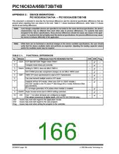
Device Differences............................................................165
Direct Addressing................................................................27
E
Electrical Characteristics...................................................113
Errata ....................................................................................3
F
FERR bit..............................................................................66
FSR Register........................................................... 17, 18, 27
G
General Description ..............................................................5
GIE bit .................................................................................93
I
I/O Ports
PORTA........................................................................29
PORTB........................................................................31
PORTC........................................................................33
PORTD..................................................................34, 37
PORTE........................................................................35
Section ........................................................................29
2
I C
Addressing ..................................................................61
Block Diagram.............................................................60
2
I C Operation ..............................................................60
Master Mode...............................................................64
Mode ...........................................................................60
Mode Selection ...........................................................60
Multi-Master Mode ......................................................64
K
KEELOQ Evaluation and Programming Tools.................... 110
Reception....................................................................62
L
Reception Timing Diagram..........................................62
SCL and SDA pins......................................................60
Slave Mode.................................................................60
Transmission...............................................................63
Loading of PC..................................................................... 26
M
MCLR............................................................................ 87, 90
Memory
2
I C (SSP Module)
Timing Diagram, Data ...............................................134
Timing Diagram, START/STOP Bits..........................134
In-Circuit Serial Programming....................................... 85, 98
INDF Register ......................................................... 17, 18, 27
Indirect Addressing .............................................................27
Instruction Cycle..................................................................14
Instruction Flow/Pipelining ..................................................14
Instruction Format ...............................................................99
Instruction Set
Data Memory .............................................................. 15
Program Memory........................................................ 15
Program Memory Maps
PIC16C73........................................................... 15
PIC16C73A......................................................... 15
PIC16C74........................................................... 15
PIC16C74A......................................................... 15
Register File Maps
PIC16C73........................................................... 16
PIC16C73A......................................................... 16
PIC16C74........................................................... 16
PIC16C74A......................................................... 16
PIC16C76........................................................... 16
PIC16C77........................................................... 16
MPLAB® Integrated Development
ADDLW .....................................................................101
ADDWF.....................................................................101
ANDLW .....................................................................101
ANDWF.....................................................................101
BCF...........................................................................101
BSF...........................................................................101
BTFSC ......................................................................102
BTFSS ......................................................................102
CALL .........................................................................102
CLRF.........................................................................102
CLRW........................................................................102
CLRWDT...................................................................102
Environment Software ...................................................... 107
DS30605C-page 170
2000 Microchip Technology Inc.

 MICROCHIP [ MICROCHIP ]