PIC12F629/675
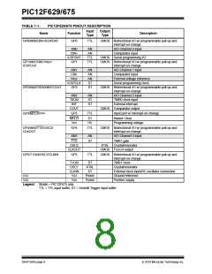
TABLE 1-1:
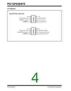
PIC12F629/675 PINOUT DESCRIPTION
Input
Type
Output
Type
Name
Function
Description
GP0/AN0/CIN+/ICSPDAT
GP0
TTL
CMOS Bidirectional I/O w/ programmable pull-up and
interrupt-on-change
AN0
CIN+
AN
AN
A/D Channel 0 input
Comparator input
ICSPDAT
GP1
TTL
TTL
CMOS Serial programming I/O
GP1/AN1/CIN-/VREF/
ICSPCLK
CMOS Bidirectional I/O w/ programmable pull-up and
interrupt-on-change
AN1
CIN-
AN
AN
AN
ST
ST
A/D Channel 1 input
Comparator input
VREF
External voltage reference
Serial programming clock
ICSPCLK
GP2
GP2/AN2/T0CKI/INT/COUT
CMOS Bidirectional I/O w/ programmable pull-up and
interrupt-on-change
AN2
T0CKI
INT
AN
ST
ST
A/D Channel 2 input
TMR0 clock input
External interrupt
COUT
CMOS Comparator output
GP3/MCLR/VPP
GP3
TTL
Input port w/ interrupt-on-change
MCLR
VPP
ST
HV
Master Clear
Programming voltage
GP4/AN3/T1G/OSC2/
CLKOUT
GP4
TTL
CMOS Bidirectional I/O w/ programmable pull-up and
interrupt-on-change
AN3
AN
ST
A/D Channel 3 input
TMR1 gate
T1G
OSC2
XTAL
Crystal/resonator
CLKOUT
CMOS FOSC/4 output
GP5/T1CKI/OSC1/CLKIN
GP5
TTL
CMOS Bidirectional I/O w/ programmable pull-up and
interrupt-on-change
T1CKI
OSC1
CLKIN
VSS
ST
TMR1 clock
XTAL
ST
Crystal/resonator
External clock input/RC oscillator connection
Ground reference
VSS
VDD
Power
Power
VDD
Positive supply
Legend: Shade = PIC12F675 only
TTL = TTL input buffer, ST = Schmitt Trigger input buffer
DS41190G-page 8
2010 Microchip Technology Inc.

 MICROCHIP [ MICROCHIP ]