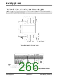
PIC12(L)F1501
Auto-shutdown Control .............................................200
Clock Source.............................................................196
Output Control...........................................................196
Selectable Input Sources..........................................196
CWGxCON0 Register .......................................................203
CWGxCON1 Register .......................................................204
CWGxCON2 Register .......................................................205
CWGxDBF Register..........................................................206
CWGxDBR Register..........................................................206
BRA .......................................................................... 216
CALL......................................................................... 217
CALLW ..................................................................... 217
LSLF ......................................................................... 219
LSRF ........................................................................ 219
MOVF ....................................................................... 219
MOVIW ..................................................................... 220
MOVLB..................................................................... 220
MOVWI..................................................................... 221
OPTION.................................................................... 221
RESET...................................................................... 221
SUBWFB .................................................................. 223
TRIS ......................................................................... 224
BCF .......................................................................... 216
BSF........................................................................... 216
BTFSC...................................................................... 216
BTFSS ...................................................................... 216
CALL......................................................................... 217
CLRF ........................................................................ 217
CLRW ....................................................................... 217
CLRWDT .................................................................. 217
COMF ....................................................................... 217
DECF........................................................................ 217
DECFSZ ................................................................... 218
GOTO ....................................................................... 218
INCF ......................................................................... 218
INCFSZ..................................................................... 218
IORLW...................................................................... 218
IORWF...................................................................... 218
MOVLW .................................................................... 220
MOVWF.................................................................... 220
NOP.......................................................................... 221
RETFIE..................................................................... 222
RETLW ..................................................................... 222
RETURN................................................................... 222
RLF........................................................................... 222
RRF .......................................................................... 223
SLEEP ...................................................................... 223
SUBLW..................................................................... 223
SUBWF..................................................................... 223
SWAPF..................................................................... 224
XORLW .................................................................... 224
XORWF .................................................................... 224
INTCON Register................................................................ 66
Internal Oscillator Block
D
DACCON0 (Digital-to-Analog Converter Control 0)
Register.....................................................................130
DACCON1 (Digital-to-Analog Converter Control 1)
Register.....................................................................130
Data Memory.......................................................................17
DC and AC Characteristics ...............................................247
DC Characteristics
Extended and Industrial ............................................234
Industrial and Extended ............................................227
Development Support .......................................................249
Device Configuration...........................................................39
Code Protection ..........................................................42
Configuration Word.....................................................39
User ID..................................................................42, 43
Device ID Register ..............................................................43
Device Overview .............................................................9, 79
Digital-to-Analog Converter (DAC)....................................127
Associated Registers ................................................130
Effects of a Reset......................................................128
Specifications............................................................245
E
Effects of Reset
PWM mode ...............................................................163
Electrical Specifications ....................................................225
Enhanced Mid-Range CPU.................................................13
Errata ....................................................................................7
Extended Instruction Set
ADDFSR ...................................................................215
F
Firmware Instructions........................................................211
Fixed Voltage Reference (FVR)........................................109
Associated Registers ................................................110
Flash Program Memory.......................................................83
Associated Registers ..................................................98
Configuration Word w/ Flash Program Memory..........98
Erasing........................................................................87
Modifying.....................................................................93
Write Verify .................................................................95
Writing.........................................................................89
Flash Program Memory Control..........................................83
FSR Register.......................................................................24
FVRCON (Fixed Voltage Reference Control) Register.....110
INTOSC
Specifications ................................................... 238
Internal Sampling Switch (RSS) Impedance...................... 124
Internet Address ............................................................... 275
Interrupt-On-Change......................................................... 105
Associated Registers................................................ 108
Interrupts............................................................................. 61
ADC .......................................................................... 118
Associated registers w/ Interrupts............................... 73
TMR1........................................................................ 149
INTOSC Specifications..................................................... 238
IOCAF Register ................................................................ 107
IOCAN Register................................................................ 107
IOCAP Register ................................................................ 107
I
INDF Register .....................................................................24
Indirect Addressing .............................................................34
Instruction Format .............................................................212
Instruction Set ...................................................................211
ADDLW .....................................................................215
ADDWF.....................................................................215
ADDWFC ..................................................................215
ANDLW .....................................................................215
ANDWF.....................................................................215
L
LATA Register .................................................................. 103
Load Conditions................................................................ 237
LSLF ................................................................................. 219
LSRF................................................................................. 219
DS41615A-page 270
Preliminary
2011 Microchip Technology Inc.

 MICROCHIP [ MICROCHIP ]