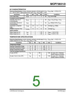
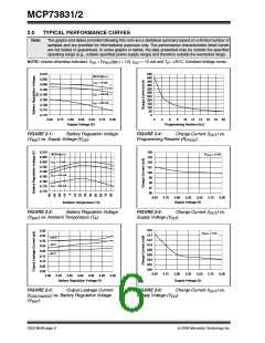
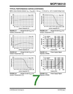
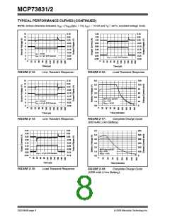
MCP73831/2
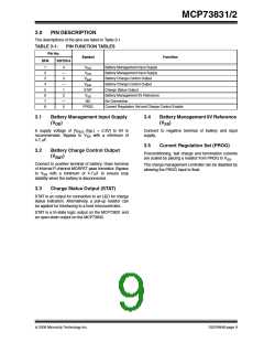
3.0
PIN DESCRIPTION
The descriptions of the pins are listed in Table 3-1.
TABLE 3-1:
PIN FUNCTION TABLES
Pin No.
Symbol
Function
DFN
SOT23-5
1
2
3
4
5
6
7
8
4
—
3
V
V
Battery Management Input Supply
Battery Management Input Supply
Battery Charge Control Output
Battery Charge Control Output
Charge Status Output
DD
DD
V
V
BAT
BAT
—
1
STAT
2
V
Battery Management 0V Reference
No Connection
SS
—
5
NC
PROG
Current Regulation Set and Charge Control Enable
3.1
Battery Management Input Supply
(V
3.4
Battery Management 0V Reference
(V
)
)
SS
DD
A supply voltage of [VREG (typ.) + 0.3V] to 6V is
recommended. Bypass to VSS with a minimum of
4.7 μF.
Connect to negative terminal of battery and input
supply.
3.5
Current Regulation Set (PROG)
3.2
Battery Charge Control Output
(V
Preconditioning, fast charge and termination currents
are scaled by placing a resistor from PROG to VSS
)
BAT
.
Connect to positive terminal of battery. Drain terminal
of internal P-channel MOSFET pass transistor. Bypass
to VSS with a minimum of 4.7 μF to ensure loop
stability when the battery is disconnected.
The charge management controller can be disabled by
allowing the PROG input to float.
3.3
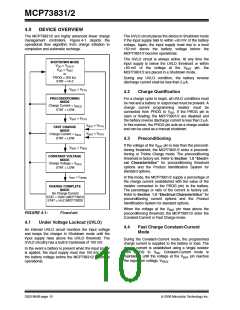
Charge Status Output (STAT)
STAT is an output for connection to an LED for charge
status indication. Alternatively, a pull-up resistor can
be applied for interfacing to a host microcontroller.
STAT is a tri-state logic output on the MCP73831 and
an open-drain output on the MCP73832.
© 2006 Microchip Technology Inc.
DS21984B-page 9

 MICROCHIP [ MICROCHIP ]