MCP414X/416X/424X/426X
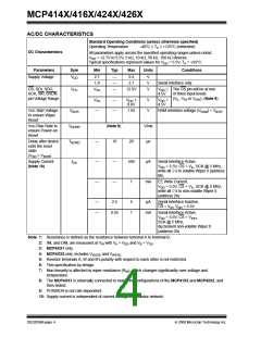
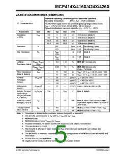
AC/DC CHARACTERISTICS
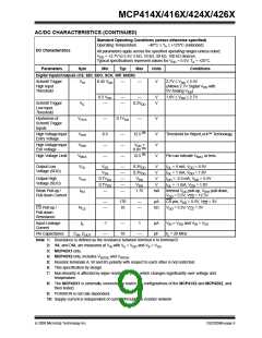
Standard Operating Conditions (unless otherwise specified)
Operating Temperature –40°C ≤ TA ≤ +125°C (extended)
DC Characteristics
All parameters apply across the specified operating ranges unless noted.
VDD = +2.7V to 5.5V, 5 kΩ, 10 kΩ, 50 kΩ, 100 kΩ devices.
Typical specifications represent values for VDD = 5.5V, TA = +25°C.
Parameters
Sym
Min
Typ
Max
Units
Conditions
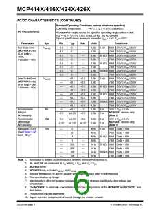
Supply Voltage
VDD
2.7
1.8
—
—
—
5.5
2.7
V
V
V
Serial Interface only.
CS, SDI, SDO,
VHV
VSS
12.5V
VDD
4.5V
≥
The CS pin will be at one
of three input levels
SCK, WP, SHDN
pin Voltage Range
(VIL, VIH or VIHH). (Note 6)
VSS
—
—
—
VDD
8.0V
+
V
V
VDD
4.5V
<
VDD Start Voltage
to ensure Wiper
Reset
VBOR
VDDRR
TBORD
1.65
RAM retention voltage (VRAM) < VBOR
VDD Rise Rate to
ensure Power-on
Reset
(Note 9)
V/ms
µs
Delay after device
exits the reset
state
—
—
—
10
20
450
1
(VDD > VBOR
)
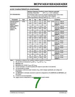
Supply Current
(Note 10)
IDD
—
—
µA
Serial Interface Active,
VDD = 5.5V, CS = VIL, SCK @ 5 MHz,
write all 0’s to volatile Wiper 0 (address
0h)
mA
EE Write Current,
VDD = 5.5V, CS = VIL, SCK @ 5 MHz,
write all 0’s to non-volatile Wiper 0
(address 2h)
—
—
2.5
5
1
µA
Serial Interface Inactive,
CS = VIH, VDD = 5.5V
0.55
mA
Serial Interface Active,
VDD = 5.5V, CS = VIHH
,
SCK @ 5 MHz,
decrement non-volatile Wiper 0
(address 2h)
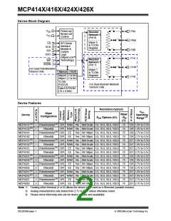
Note 1: Resistance is defined as the resistance between terminal A to terminal B.
2: INL and DNL are measured at VW with VA = VDD and VB = VSS
.
3: MCP4XX1 only.
4: MCP4XX2 only, includes VWZSE and VWFSE
.
5: Resistor terminals A, W and B’s polarity with respect to each other is not restricted.
6: This specification by design.
7: Non-linearity is affected by wiper resistance (RW), which changes significantly over voltage and
temperature.
8: The MCP4XX1 is externally connected to match the configurations of the MCP41X2 and MCP42X2, and
then tested.
9: POR/BOR is not rate dependent.
10: Supply current is independent of current through the resistor network
DS22059B-page 4
© 2008 Microchip Technology Inc.

 MICROCHIP [ MICROCHIP ]