dsPIC33F/PIC24H PROGRAMMING SPECIFICATION
2.3
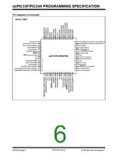
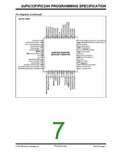
Pin Diagrams
The pin diagrams for the dsPIC33F/PIC24H device
family are shown in the following figures. The pins that
are required for programming are listed in Table 2-1.
The MCLR, PGC1, PGD1, PGC2, PGD2, PGC3 and
PGD3 pins are shown in bold letters in the figures.
Refer to the appropriate device data sheet for complete
pin descriptions.
TABLE 2-1:
Pin Name
PIN DESCRIPTIONS (PINS USED DURING PROGRAMMING)
During Programming
Pin Description
Pin Name
Pin Type
MCLR
MCLR
VDD
P
P
Programming Enable
(1)
VDD and AVDD
Power Supply
(1)
VSS and AVSS
VDDCORE
PGC1
VSS
P
Ground
VDDCORE
PGC1
PGD1
PGC2
PGD2
PGC3
PGD3
P
Regulated Power Supply for Core
Primary Programming Pin Pair: Serial Clock
Primary Programming Pin Pair: Serial Data
Secondary Programming Pin Pair: Serial Clock
Secondary Programming Pin Pair: Serial Data
Tertiary Programming Pin Pair: Serial Clock
Tertiary Programming Pin Pair: Serial Data
I
PGD1
I/O
I
PGC2
PGD2
I/O
I
PGC3
PGD3
I/O
Legend: I = Input, O = Output, P = Power
Note 1: All power supply and ground pins must be connected, including analog supplies (AVDD) and ground
(AVSS).
© 2007 Microchip Technology Inc.
Preliminary
DS70152D-page 3

 MICROCHIP [ MICROCHIP ]