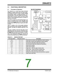
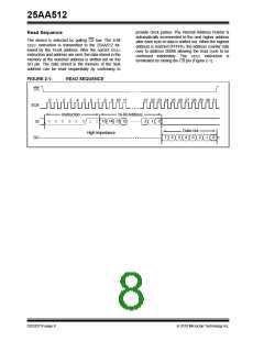
25AA512
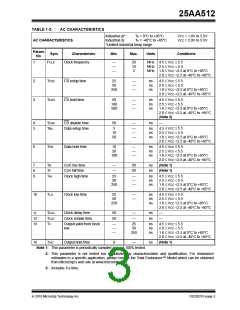
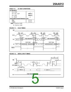
TABLE 1-2:
AC CHARACTERISTICS
Industrial (I)*:
Industrial (I):
TA = 0°C to +85°C
TA = -40°C to +85°C
VCC = 1.8V to 5.5V
VCC = 2.0V to 5.5V
AC CHARACTERISTICS
*Limited industrial temp range.
Param.
Sym.
No.
Characteristic
Clock frequency
Min.
Max.
Units
Conditions
1
2
3
FCLK
TCSS
TCSH
—
—
—
20
10
2
MHz 4.5 VCC 5.5
MHz 2.5 VCC 5.5
MHz 1.8 VCC <2.5 at 0°C to +85°C
2.0 VCC <2.5 at -40°C to +85°C
CS setup time
CS hold time
25
50
250
—
—
—
ns
ns
ns
4.5 VCC 5.5
2.5 VCC 5.5
1.8 VCC <2.5 at 0°C to +85°C
2.0 VCC <2.5 at -40°C to +85°C
50
100
500
—
—
—
ns
ns
ns
4.5 VCC 5.5
2.5 VCC 5.5
1.8 VCC <2.5 at 0°C to +85°C
2.0 VCC <2.5 at -40°C to +85°C
(Note 3)
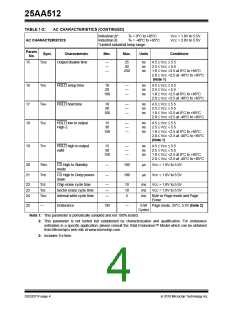
4
5
TCSD
Tsu
CS disable time
Data setup time
50
—
ns
—
5
10
50
—
—
—
ns
ns
ns
4.5 VCC 5.5
2.5 VCC 5.5
1.8 VCC <2.5 at 0°C to +85°C
2.0 VCC <2.5 at -40°C to +85°C
6
THD
Data hold time
10
20
100
—
—
—
ns
ns
ns
4.5 VCC 5.5
2.5 VCC 5.5
1.8 VCC <2.5 at 0°C to +85°C
2.0 VCC <2.5 at -40°C to +85°C
7
8
9
TR
TF
CLK rise time
CLK fall time
Clock high time
—
—
20
20
ns
ns
(Note 1)
(Note 1)
THI
25
50
250
—
—
—
ns
ns
ns
4.5 VCC 5.5
2.5 VCC 5.5
1.8 VCC <2.5 at 0°C to +85°C
2.0 VCC <2.5 at -40°C to +85°C
10
TLO
Clock low time
25
50
250
—
—
ns
ns
ns
4.5 VCC 5.5
2.5 VCC 5.5
1.8 VCC <2.5 at 0°C to +85°C
2.0 VCC <2.5 at -40°C to +85°C
11
12
13
TCLD
TCLE
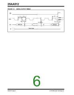
TV
Clock delay time
Clock enable time
50
50
—
—
ns
ns
—
—
Output valid from clock
low
—
—
—
25
50
250
ns
ns
ns
4.5 VCC 5.5
2.8 VCC 5.5
1.8 VCC <2.5 at 0°C to +85°C
2.0 VCC <2.5 at -40°C to +85°C
14
THO
Output hold time
0
—
ns
(Note 1)
Note 1: This parameter is periodically sampled and not 100% tested.
2: This parameter is not tested but established by characterization and qualification. For endurance
estimates in a specific application, please consult the Total Endurance™ Model which can be obtained
from Microchip’s web site at www.microchip.com.
3: Includes THI time.
2010 Microchip Technology Inc.
DS22021F-page 3

 MICROCHIP [ MICROCHIP ]