ML4901
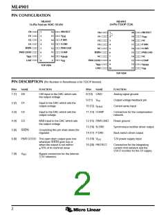
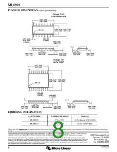
PIN CONFIGURATION
ML4901
20-Pin TSSOP (T20)
ML4901
16-Pin Narrow SOIC (S16N)
D0
D1
16
15
14
13
12
11
10
9
PROTECT
1
2
3
4
5
6
7
8
D0
1
2
20
PROTECT
V
DD
D1
19
18
17
16
15
14
13
12
11
V
DD
D2
P DRV
D2
D3
3
NC
D3
N DRV
4
P DRV
N DRV
PWR GND
NC
SHDN
PWR GOOD
PWR GND
COMP
NC
5
SHDN
NC
6
V
I
7
REF
SENSE
PWR GOOD
8
COMP
GND
V
FB
V
9
I
SENSE
REF
GND
TOP VIEW
10
V
FB
TOP VIEW
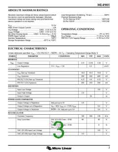
PIN DESCRIPTION (Pin Number in Parentheses is for TSSOP Version)
PIN#
NAME
FUNCTION
PIN#
NAME
FUNCTION
1 (1)
D0
LSB input to the DAC which sets
the output voltage
8 (10) GND
Analog signal ground
9 (11)
V
Output voltage feedback pin
Current sense input
FB
2 (2)
3 (3)
4 (4)
5 (6)
6 (8)
D1
Input to the DAC which sets the
output voltage
10 (12) I
SENSE
D2
Input to the DAC which sets the
output voltage
11 (13) COMP
Connection for the compensation
network
D3
MSB input to the DAC which sets
the output voltage
12 (15) PWR GND
13 (16) N DRV
14 (17) P DRV
Power ground
Synchronous rectifier driver output
Buck switch driver output
12V power supply input
SHDN
Grounding this pin shuts down the
regulator
PWR GOOD This open drain output goes low
whenever SHDN goes low or
15 (19) V
DD
when the output is not within
+10% of its nominal value
16 (20) PROTECT
Connection for the integrating
current limit network and the
UVLO monitor for the 5V supply
7 (9)
V
REF
Bypass connection for the internal
3.5V reference
2

 MICRO-LINEAR [ MICRO LINEAR CORPORATION ]