ML4827
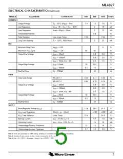
ELECTRICAL CHARACTERISTICS (Continued)
SYMBOL
PARAMETER
CONDITIONS
MIN
TYP
MAX
UNITS
REFERENCE
Output Voltage
TA = 25°C, I(VREF) = 1mA
VCCZ - 3V < VCC < VCCZ - 0.5V
1mA < I(VREF) < 20mA
7.4
7.5
2
7.6
10
15
V
mV
mV
%
Line Regulation
Load Regulation
Temperature Stability
Total Variation
2
0.4
Line, Load, Temp
7.35
7.65
25
V
Long Term Stability
TJ = 125°C, 1000 Hours
5
mV
PFC
Minimum Duty Cycle
Maximum Duty Cycle
Output Low Voltage
VIEAO > 4.0V
0
%
%
V
V
V
V
V
ns
VIEAO < 1.2V
90
95
0.4
0.8
0.7
10.5
10
IOUT = -20mA
IOUT = -100mA
IOUT = 10mA, VCC = 8V
IOUT = 20mA
0.8
2.0
1.5
Output High Voltage
Rise/FallTime
10
IOUT = 100mA
CL = 1000pF
9.5
50
PWM
Duty Cycle Range
Output Low Voltage
ML4827-1
0-44
0-64
0-47
0-70
0.4
0-50
0-74
0.8
%
%
V
V
V
V
V
ns
ML4827-2
IOUT = -20mA
IOUT = -100mA
IOUT = 10mA, VCC = 8V
IOUT = 20mA
IOUT = 100mA
CL = 1000pF
0.8
2.0
0.7
1.5
Output High Voltage
Rise/FallTime
10
10.5
10
9.5
50
SUPPLY
Shunt Regulator Voltage (VCCZ
VCCZ Load Regulation
VCCZ Total Variation
Start-up Current
)
12.8
12.4
13.5
14.2
±300
14.6
1.0
V
mV
V
25mA < ICC < 55mA
Load, Temp
±100
VCC = 11.8V, CL = 0
VCC < VCCZ - 0.5V, CL = 0
0.7
16
mA
mA
V
Operating Current
19
Undervoltage Lockout Threshold
Undervoltage Lockout Hysteresis
12
13
14
2.7
3.0
3.3
V
Note 1: Limits are guaranteed by 100% testing, sampling, or correlation with worst-case test conditions.
Note 2: Includes all bias currents to other circuits connected to the VFB pin.
Note 3: Gain = K x 5.3V; K = (IGAINMOD - IOFFSET) x IAC x (VEAO - 1.5V)-1
.
5

 MICRO-LINEAR [ MICRO LINEAR CORPORATION ]