Micrel
SY88993AV
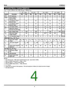
AC ELECTRICAL CHARACTERISTICS
V
= +3.3V ±10% or +5V ±10%, R
= 50Ω to V
LOAD CC
CC
TA = –40°C
Min. Max.
TA = 0°C
TA = +25°C
TA = +85°C
Symbol
HYS
Parameter
Min.
2
Max.
8
Min.
2
Typ.
4.6
35
Max.
8
Min.
2
Max.
8
Unit
dB
LOS Hysteresis
2
8
PSRR
Power Supply(1)
Rejection Ratio
—
—
—
—
—
—
—
—
—
—
dB
tOFFL
tOFFH
LOS Release Time(2)
Minimum Input
0.5
0.5
—
—
0.5
0.5
—
—
0.1
0.1
0.5
0.5
—
—
0.5
0.5
µs
µs
LOS Release Time(2)
Maximum Input
tONL
tr, tf
LOS Assert Time(2)
—
—
0.5
—
—
0.5
—
—
0.2
60
0.5
—
—
0.5
µs
Differential Output(3)
Rise/Fall Time (20%-80%)
120
120
120
120
ps
VID
Input Voltage Range
4
1800
600
4
1800
600
4
—
1800
1200
4
1800 mVp-p
VOD
Differential Output
Voltage Swing(4)
—
—
—
800(5)
600
—
mVp-p
VSR
LOS Sensitivity Range
4
50
4
50
4
—
50
4
50
mVp-p
Output Spec (DOUT and /DOUT
)
VOH
VOL
ZO
HIGH Level Output
Voltage
VCC –20 VCC
VCC –20
—
VCC
VCC –20 VCC –5
VCC
VCC –20
—
VCC
mV
LOW Level Output(6)
ß
—
V
–300
V
–300
—
V
–400
V
–300
V
–300 mV
CC
CC
CC
CC
CC
Single-Ended Output(7)
Impedance
40
60
40
60
40
50
60
40
60
Ω
Input Spec (DIN and /DIN)
AV(Diff)
Differential Voltage
Gain
—
—
—
—
—
39
—
—
—
dB
B–3dB
S21
3dB Bandwidth
—
—
—
—
—
—
—
2.5
33
—
—
—
—
—
GHz
dB
Single-Ended Small
Signal-Gain
26
26
26
26
NOTES:
1. Input referred noise = RMS output noise/low frequency gain. Input referred, 55MHz.
2. Input is a 200MHz square wave, tr < 300ps, 1.8Vp-p.
3. With input signal VID > 50mVp-p with 50Ω load.
4. Input is a 200MHz square wave, tr < 300ps, 50Ω load.
5. VID > 5mVp-p.
6. Output levels are based on 50Ω impedance. If the load impedance is different, the output level will be changed.
7. See output structure.
4

 MICREL [ MICREL SEMICONDUCTOR ]