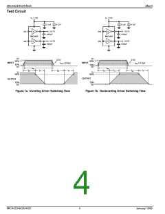
MIC4423/4424/4425
= 12 x [(0.5 x 0.0035) + (0.5 x 0.0003)]
Micrel
= 0.213W
= 0.0228W
In a ceramic package with an θ of 100°C/W, this amount of
JA
Total power dissipation, then, is:
power results in a junction temperature given the maximum
40°C ambient of:
P
= 0.2160 + 0.0066 + 0.0228
= 0.2454W
D
(0.213 x 100) + 40 = 61.4°C
Assuming an SOIC package, with an θ of 120°C/W, this will The actual junction temperature will be lower than calculated
JA
result in the junction running at:
both because duty cycle is less than 100% and because the
graph lists R at a T of 125°C and the R at 61°C
T will be somewhat lower.
J
DS(on)
J
DS(on)
0.2454 x 120 = 29.4°C
aboveambient,which,givenamaximumambienttemperature
of 60°C, will result in a maximum junction temperature of
89.4°C.
Definitions
C = Load Capacitance in Farads.
L
D = Duty Cycle expressed as the fraction of time the input
to the driver is high.
EXAMPLE 2: A MIC4424 operating on a 15V input, with one
driver driving a 50Ω resistive load at 1MHz, with a duty cycle
of67%, andtheotherdriverquiescent, inamaximumambient
temperature of 40°C:
f = Operating Frequency of the driver in Hertz
I = Power supply current drawn by a driver when both
H
2
P = I x R x D
L
O
inputs are high and neither output is loaded.
First, I must be determined.
O
I = Power supply current drawn by a driver when both
L
inputs are low and neither output is loaded.
I
O
= V / (R + R
)
S
O
LOAD
I = Output current from a driver in Amps.
D
Given R from the characteristic curves then,
O
P = Total power dissipated in a driver in Watts.
D
I
= 15 / (3.3 + 50)
= 0.281A
O
P = Power dissipated in the driver due to the driver’s load
L
I
O
in Watts.
and:
P
= Power dissipated in a quiescent driver in Watts.
Q
2
P
L
= (0.281) x 3.3 x 0.67
P = Powerdissipatedinadriverwhentheoutputchanges
T
= 0.174W
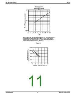
states (“shoot-through current”) in Watts. NOTE: The
“shoot-through” current from a dual transition (once
up, once down) for both drivers is stated in the graph
on the following page in ampere-nanoseconds. This
figure must be multiplied by the number of repetitions
per second (frequency to find Watts).
P
= F x V x (A•s)/2
T
S
(because only one side is operating)
–9
= (1,000,000 x 15 x 3.3 x 10 ) / 2
= 0.025 W
and:
R = Output resistance of a driver in Ohms.
P
Q
= 15 x [(0.67 x 0.00125) + (0.33 x 0.000125) +
(1 x 0.000125)]
O
V = Power supply voltage to the IC in Volts.
S
(this assumes that the unused side of the driver has its input
grounded, which is more efficient)
= 0.015W
then:
P
= 0.174 + 0.025 + 0.0150
D
MIC4423/4424/4425
10
January 1999

 MICREL [ MICREL SEMICONDUCTOR ]