MIC39300/39301
Micrel
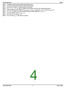
Note 1. Exceeding the absolute maximum ratings may damage the device.
Note 2. The device is not guaranteed to function outside its operating rating.
Note 3. Devices are ESD sensitive. Handling precautions recommended.
Note 4.
P
= (T
– T ) ÷ θ , where θ depends upon the printed circuit layout. See “Applications Information.”
J(max) A JA JA
D(max)
Note 5. Output voltage temperature coefficient is ∆V
÷ (T
– T
) where T
is +125°C and T
is 0°C.
OUT(worst case)
J(max)
J(min)
J(max)
J(min)
Note 6.
Note 7.
Note 8.
V
I
= V – V
when V
decreases to 99% of its nominal output voltage with V = V + 1V.
OUT
DO
IN
OUT
OUT
IN
is the quiescent current. I = I
+ I
.
GND
IN
GND
OUT
V
≤ 0.8V, V ≤ 8V, and V
= 0V
EN
IN
OUT
Note 9. For a 2.5V device, V = 2.250V (device is in dropout).
IN
MIC39300/39301
4
March 2000

 MICREL [ MICREL SEMICONDUCTOR ]