Micrel, Inc.
MIC37139
Absolute Maximum Ratings(1)
Operating Ratings(2)
Supply Voltage (VIN)......................................................6.5V
Enable Input Voltage (VEN)............................................6.5V
Power Dissipation .....................................Internally Limited
Junction Temperature (TJ) ..................–40°C ≤ TJ ≤ +125°C
Lead Temperature (soldering, 5 sec.)........................ 260°C
Storage Temperature (Ts) ...................–65°C ≤ TJ ≤ +150°C
ESD Rating(3)
Supply Voltage (VIN)....................................... 2.25V to 6.0V
Enable Input Voltage (VEN).................................. 0V to 6.0V
Junction Temperature (TJ) ..................–40°C ≤ TJ ≤ +125°C
Maximum Power Dissipation(4)
Package Thermal Resistance
SOT-223 (θJC)....................................................50°C/W
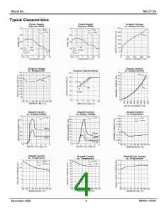
Electrical Characteristics(5)
TA = 25°C with VIN = VOUT + 1V; VEN = VIN; bold values indicate –40°C< TJ < +125°C, unless noted.
Parameter
Condition
Min
–1
Typ
Max
+1
Units
%
Output Voltage Accuracy
IL = 10mA
10mA < IOUT < IL(max), VOUT + 1 ≤ VIN ≤ 6V
VIN = VOUT +1.0V to 6.0V
IL = 10mA to 1.5A
IL = 750mA
–2
+2
%
Output Voltage Line Regulation
Output Voltage Load Regulation
VIN – VOUT; Dropout Voltage(6)
0.06
0.2
0.5
1
%
%
350
500
30
mV
mV
mA
µA
A
IL = 1.5A
Ground Pin Current(7)
Ground Pin Current in Shutdown
Current Limit
IL = 1.5A
17
1.0
VIL ≤ 0.5V, VIN = VOUT + 1V
VOUT = 0
2.25
4
Notes:
1. Exceeding the absolute maximum rating may damage the device.
2. The device is not guaranteed to function outside its operating rating.
3. Devices are ESD sensitive. Handling precautions recommended.
4. PD(max) = (TJ(max) – TA) ÷ θJA, where θJA, depends upon the printed circuit layout. See “Applications Information.”
5. Specification for packaged product only.
6. VDO = VIN – VOUT when VOUT decreased to 98% of its nominal output voltage with VIN = VOUT +1V. For output voltages below 1.75V, dropout voltage
specification does not apply due to a minimum input operating voltage of 2.25V.
7. IGND is the quiescent current. IIN = IGND + IOUT
.
M9999-110209
November 2009
3

 MICREL [ MICREL SEMICONDUCTOR ]