MIC37100/37101/37102
Micrel
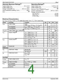
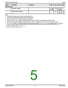
Symbol
Parameter
Condition
Min
Typ
Max
Units
MIC37102 Only
Reference Voltage
1.228 1.240 1.252
V
V
1.215
1.265
Adjust Pin Bias Current
40
80
120
nA
nA
Notes:
1. Exceeding the absolute maximum ratings may damage the device.
2. The device is not guaranteed to function outside its operating rating.
3. Devices are ESD sensitive. Handling precautions recommended.
4. P (max) = (T (max) – T ) ÷ θ , where θ depends upon the printed circuit layout. See “Applications Information” section.
D
J
A
JA
JA
5. Output voltage temperature coefficient is ∆V
(worst case) ÷ (T (max) – T (min)) where T (max) is +125°C and T (min) is –40°C.
OUT
J
J
J
J
6.
V
= V – V
when V
decreases to 98% of its nominal output voltage with V = V
+ 1V. For output voltages below 2.25V, dropout
DO
IN
OUT
OUT
IN
OUT
voltage is the input-to-output voltage differential with the minimum input voltage being 2.25V. Minimum input operating voltage is 2.25V.
7.
8.
I
is the quiescent current. I = I + I
.
OUT
GND
IN
GND
V
≤ 0.8V, V ≤ 6V, and V
= 0V.
EN
IN
OUT
September 2004
5
M9999-091604

 MICREL [ MICREL SEMICONDUCTOR ]