Micrel
MIC2586/MIC2586R
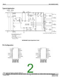
Pin Description
Pin Number
Pin Name
Pin Function
1
8
NC
Reserved: Make no external connections to these pins.
12
2
ON
Enable Input: When the voltage at the ON pin is higher than the VONH threshold,
a start cycle is initiated. An internal current source (IGATEON) is activated which
charges the GATE pin, ramping up the voltage at this pin to turn on an external
MOSFET. Whenever the voltage at the ON pin is lower than the VONL threshold,
an undervoltage lockout condition is detected and the IGATEON current source is
disabled while the GATE pin is pulled low by another internal current source
(IGATEOFF). After a load current fault, toggling the ON pin LOW will reset the
circuit breaker then back HIGH (ON pin) will initiate another start cycle.
3
FB
Output Voltage Feedback Input: This pin is connected to an external resistor
divider that is used to sample the output load voltage. The voltage at this pin is
measured against an internal comparator whose output controls the PWRGD (or
/PWRGD) signal. PWRGD (or /PWRGD) asserts when the FB pin voltage
crosses the VFBH threshold. When the FB pin voltage is lower than its VFBL
threshold, PWRGD (or /PWRGD) is deasserted. The FB comparator exhibits a
typical hysteresis of 80mV.
The FB pin voltage also affects the MIC2586/MIC2586R’s foldback current limit
operation (see the “Functional Description” section for further information).
4
PWRGD1
(MIC2586-1)
(MIC2586R-1)
Active-HIGH
Power-is-Good (PWRGD1 or /PWRGD1), Open-drain Output: This pin remains
deasserted during start up while the FB pin voltage is below the VFBH threshold.
Once the voltage at the FB pin rises above the VFBH threshold, the Power-is-
Good output asserts with minimal delay (typically ≤ 5µs).
For the (-1) options, the PWRGDx output pin will be high-impedance when the
FB pin voltage is higher than VFBH and will pull down to GND when the FB pin
/PWRGD1
(MIC2586-2)
voltage is less than VFBL
.
For the (-2) options, the /PWRGDx output pin will be high-impedance when the
FB pin voltage is lower than VFBL and will pull down to GND when the FB pin
(MIC2586R-2)
Active-LOW
voltage is higher than VFBH
.
Each Power-is-Good output pin is connected to an open-drain, N-channel
transistor implemented with high-voltage structures. These transistors are
capable of operating with pull-up resistors to supply voltages as high as 100V.
To use this signal as a logic control in low-voltage dc-dc conversion applications,
an external pull-up resistor between this pin and the logic supply voltage is
recommended, unless an internal pull-up impedance is provided by the dc-dc
module or other device (load).
5
PWRGD2
(MIC2586-1)
(MIC2586R-1)
Active-HIGH
Power-is-Good 2 (PWRGD2 or /PWRGD2), Open-drain Output: For the (-1)
option, this output signal is asserted when the following is true: PWRGD1 =
Asserted AND the PWRGD1-to-PWRGD2 delay (tPG(1-2)) has elapsed, where
t
PG(1-2) is the time delay programmed by the capacitor (CPG) connected to the
PGTIMER pin. Once PWRGD1 is asserted, an internal current source (ICPG
begins to charge CPG. When the voltage on CPG crosses the VPG2 threshold
)
/PWRGD2
(MIC2586-2)
(typically, 0.625V), PWRGD2 is asserted. The same description above applies
to the (-2) option. For further information, refer to the PWRGD1 and PGTIMER
pin descriptions.
(MIC2586R-2)
Active-LOW
To use this signal as a logic control in low-voltage dc-dc conversion applications,
an external pull-up resistor between this pin and the logic supply voltage is
recommended, unless an internal pull-up impedance is provided by the dc-dc
module or other device (load).
6
GND
Tie this pin directly to the system’s analog GND plane
M9999-102204
(408) 955-1690
October 2004
3

 MICREL [ MICREL SEMICONDUCTOR ]