MIC2546/2547
Micrel
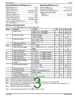
Absolute Maximum Ratings (Note 1)
Operating Ratings (Note 2)
Supply Voltage (V ) ..................................................+6.0V
Supply Voltage (V ) ................................... +2.7V to +5.5V
IN
IN
Output Voltage (V
Output Current (I
) ...............................................+6.0V
Current Limit Set Range.....................................0.1 to 1.5A
OUT
) ............................... Internally Limited
Ambient Temperature Range (T ) ............. –40°C to +85°C
OUT
A
Enable Input (V ) ................................ –0.3V to V +0.3V
Package Thermal Resistance
EN
IN
SOP (θ ) ..........................................................120°C/W
Fault Flag Voltage (V
)...........................................+6.0V
JA
FLG
TSSOP (θ ) .....................................................100°C/W
JA
Fault Flag Current (I
) ............................................50mA
FLG
Storage Temperature (T ) ....................... –65°C to +150°C
S
Junction Temperature (T ) ....................... Internally Limited
J
Lead Temperature (soldering 5 sec.) ........................ 260°C
ESD Rating, Note 3 ...................................................... 2kV
Electrical Characteristics
VIN = +5V; TA = 25°C, bold indicates –40°C to +85°C; unless noted
Symbol
Parameter
Condition
Min
2.4
Typ
1.5
200
1.7
1.5
.01
.01
1
Max
10
Units
µA
µA
V
Supply Current
Switch off, OUT = open, Note 4
Switch on, OUT = open, Note 4
Enable High, Note 4
Enable Low, Note 4
VEN = VOH(min) = 2.4V
VEN = VOL(max) = 0.8V
Note 5
320
VEN
Enable Input Voltage
Enable Input Current
0.8
1
V
µA
µA
pF
mΩ
V
1
Enable Input Capacitance
Switch Resistance
RDS(on)
IOUT = 500mA
80
120
Current Limit Factor, Note 6
IOUT = 100mA to 1.5A, VOUT = 1.0V to 4.0V,
184
230
276
Note 6
Output Leakage Current
Output Turn-On Delay
Output Turn-On Rise Time
Output Turnoff Delay
Switch off
1
2
10
5
µA
ms
ms
µs
µs
°C
°C
Ω
tON
tR
tOFF
tF
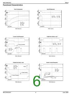
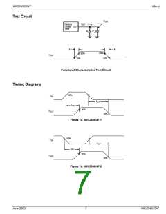
RL = 10Ω, CL = 1µF, Figure 1a and 1b
RL = 10Ω, CL = 1µF, Figure 1a and 1b
RL = 10Ω, CL = 1µF, Figure 1a and 1b
RL = 10Ω, CL = 1µF, Figure 1a and 1b
TJ increasing
1
1
2
5
22
21
140
130
4
Output Turnoff Fall Time
Overtemperature Threshold
Shutdown
TJ decreasing
Error Flag Output Resistance
VIN = 5V, IL = 10µA
15
20
1
VIN = 3.3V, IL = 10µA
5
Ω
Error Flag Off Current
VFLG = 5V
0.01
µA
µs
µs
µs
µs
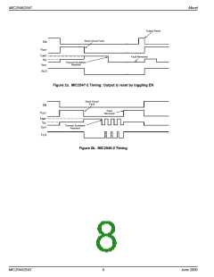
EN Pulse Reset Width
MIC2547 Thermal Shutdown Latch
MIC2547, Note 5
5
0
VIN to EN Set-Up
Current-Limit Response Time
Overcurrent FLG Response Time
VOUT = 0V
25
5
VOUT = VIN/2 to FLG low
Note 1. Exceeding the absolute maximum rating may damage the device.
Note 2. The device is not guaranteed to function outside its operating rating.
Note 3. Devices are ESD sensitive. Handling precautions recommended. Human body model, 1.5k in series with 100pF.
Note 4. Off is ≤ 0.8V and on is ≥ 2.4V for the MIC2546-1 and MIC2547-1. Off is ≥ 2.4V and on is ≤ 0.8V for the MIC2546-2 and MIC2547-2. The
enable input has about 200mV of hysteresis.
Note 5. Guaranteed by design, but not production tested.
230V
I
=
LIMIT
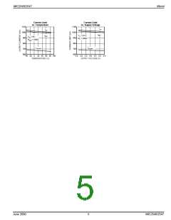
Note 6. Current limit threshold is determined by:
, where R
is in ohms.
SET
R
SET
June 2000
3
MIC2546/2547

 MICREL [ MICREL SEMICONDUCTOR ]