MIC2536
Micrel
Absolute Maximum Ratings (Note 1)
Operating Ratings (Note 2)
Supply Voltage (V ) .....................................................+6V
Supply Voltage (V ) ................................... +2.7V to +5.5V
IN
IN
Fault Flag Voltage (V
Fault Flag Current (I
)..............................................+6V
Ambient Operating Temperature (T ) ........ –40°C to +85°C
FLG
A
) ............................................25mA
) ..................................................+6V
Thermal Resistance
FLG
OUT
SOP (θ ) ..........................................................160°C/W
Output Voltage (V
Output Current (I
JA
MSOP (θ ) .......................................................206°C/W
) ............................... Internally Limited
JA
OUT
Control Input (V ) ................................... –0.3V to V +2V
EN
IN
Storage Temperature (T ) ....................... –65°C to +150°C
S
Lead Temperature (Soldering 5 sec.) ....................... 260°C
ESD Rating, Note 3 ...................................................... 1kV
Electrical Characteristics
VIN = +5V; TA = 25°C, bold values indicate –40°C ≤ TA ≤ +85°C; unless noted
Parameter
Condition
Min
Typ
0.75
60
Max
5
Units
µA
µA
V
Supply Current
both switches off, OUTA–B = open, Note 4
both switches on, OUTA–B = open, Note 4
low-to-high transition, Note 4
high-to-low transition, Note 4
VEN = 0V to 5.5V
100
2.4
Enable Input Threshold
1.7
1.5
0.01
1
0.8
V
Enable Input Current
1
µA
pF
mΩ
ms
ms
µs
Enable Input Capacitance
Switch Resistance
Note 5
single switch, IOUT = 100mA
RL = 50Ω, CL = 1µF
400
1.5
1.4
130
115
1
700
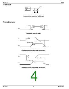
Output Turn-On Delay, tON
Output Turn-On Rise Time, tR
Output Turnoff Delay, tOFF
Output Turnoff Fall Time, tF
Output Leakage Current
Current Limit Threshold
Short Circuit Current Limit
Current Limit Response
Flag Response Delay, tD
RL = 50Ω, CL = 1µF
RL = 50Ω, CL = 1µF
RL = 50Ω, CL = 1µF
µs
each output (switch off)
10
µA
mA
mA
µs
ramped load applied to enable output
each output (enabled into load), VOUT = 0V
VOUT = 0V to IOUT = ILIMIT (short applied to output), Note 5
VIN = 5V, apply VOUT = 0V until FLG low
VIN = 3.3V, apply VOUT = 0V until FLG low
TJ increasing, Note 5
500
400
150
5
275
10
13
20
ms
ms
°C
°C
Ω
13
Overtemperature Shutdown
Threshold
135
125
10
TJ decreasing, Note 5
Error Flag Output Resistance
VIN = 5V, IL = 10mA
20
30
1
VIN = 3.3V, IL = 10mA
15
Ω
Error Flag Off Current
VFLAG = 5V
0.01
µA
Note 1. Exceeding the absolute maximum rating may damage the device.
Note 2. The device is not guaranteed to function outside its operating rating.
Note 3. Devices are ESD sensitive. Handling precautions recommended. Human body model, 1.5kΩ in series with 100pF.
Note 4. Off is ≤ 0.8V and on is ≥ 2.4V for the MIC2536-1. Off is ≥ 2.4V and on is ≤ 0.8V for the MIC2536-2. The enable input has approximately
200mV of hysteresis.
Note 5. Guaranteed by design. Not production tested.
March 2000
3
MIC2536

 MICREL [ MICREL SEMICONDUCTOR ]