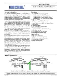
MIC2505/2506
Micrel
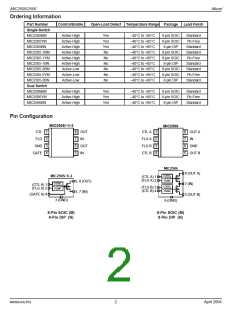
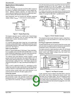
Pin Description
Pin Number
Pin Number
Pin Name
Pin Function
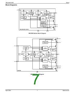
MIC2505 series
MIC2506
1
2
1 / 4
CTL (A/B)
Control (Input): TTL compatible control input. High input typically > 1.8V.
Low input typically < 1.6V. MIC2505, MIC2505-1 and MIC2506 are active
high. MIC2505-2 is active low.
2 / 3
FLG (A/B)
Fault Flag (Output): Active-low, open-drain output. If CTL is low, indicates
open load. If CTL is high, indicates current limit, thermal shutdown, or
UVLO.
MIC2505-1 and -2 do not support open-load detect.
3
4
6
GND
Ground: Return.
—
GATE
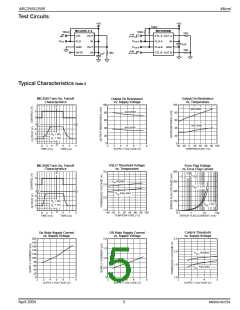
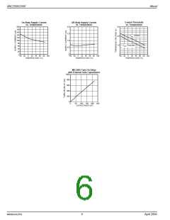
Output MOSFET Gate: Open for fastest rise time. Connect capacitor to
ground to slow rise time. (See MIC2505 Turn-On Delay graph)
5, 7
6, 8
7
IN
Supply Input: Output MOSFET drain. Also supplies IC’s internal circuitry.
Connect to supply.
MIC2505 series only: Pins 5 and 7 must be externally connected together.
8 / 5
OUT (A/B)
Switch Output: Output MOSFET source. Typically connect to switched side
of load. Output voltage can be pulled above input voltage in off mode.
MIC2505 series only: Pins 6 and 8 must be externally connected together.
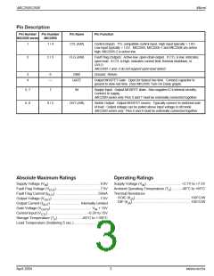
Absolute Maximum Ratings
Operating Ratings
Supply Voltage (V ) ....................................................8.0V
Supply Voltage (V ) ................................... +2.7V to +7.5V
IN
IN
Fault Flag Voltage (V
Fault Flag Current (I
).............................................7.5V
Ambient Operating Temperature (T ) ........ –40°C to +85°C
FLG
A
) ............................................50mA
) .................................................7.5V
Thermal Resistance
FLG
SOIC (θ ) .........................................................160°C/W
Output Voltage (V
Output Current (I
JA
OUT
DIP (θ )............................................................105°C/W
JA
) ............................... Internally Limited
OUT
Gate Voltage (V
Control Input (V
) ......................................... V + 15V
GATE
IN
) ....................................... –0.3V to 15V
CTL
Storage Temperature (T ) ....................... –65°C to +150°C
A
Lead Temperature (Soldering 5 sec.) ....................... 260°C
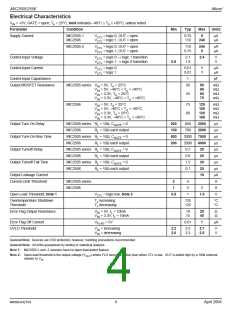
April 2004
3
M9999-042704

 MICREL [ MICREL SEMICONDUCTOR ]