MIC2042/2043
Micrel
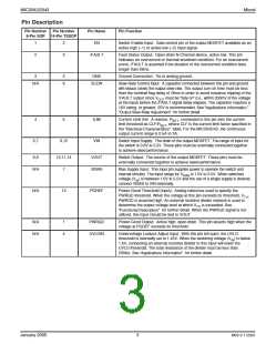
Pin Description
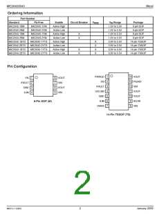
Pin Number Pin Number
8-Pin SOP 14-Pin TSSOP
Pin Name
EN
Pin Function
1
2
Switch Enable Input: Gate control pin of the output MOSFET available as an
active high (–1) or active low (–2) input signal.
2
3
/FAULT
Fault Status Output: Open-drain N-Channel device, active low. This pin
indicates an overcurrent or thermal shutdown condition. For an overcurrent
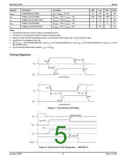
event, /FAULT is asserted if the duration of the overcurrent condition lasts
longer than 28ms.
3
5
9
GND
Ground Connection: Tie to analog ground.
N/A
SLEW
Slew-Rate Control Input: A capacitor connected between this pin and ground
will reduce (slow) the output slew-rate. The output turn-on time must be less
than the nominal flag delay of 28ms in order to avoid nuisance tripping of the
/FAULT output since VOUT must be “fully on” (i.e., within 200mV of the voltage
at the input) before the /FAULT signal delay elapses. The capacitor requires a
16V rating, or greater, 25V is recommended. See “Applications Information,”
“Output Slew-Rate Adjustment” for further detail.
4
6
ILIM
VIN
Current Limit Set: A resistor, RSET, connected to this pin sets the current
limit threshold as CLF/RSET, where CLF is the current limit factor specified in
the “Electrical Characteristics” table. For the MIC2042/43, the continuous
output current range is 0.5A to 3A.
5,7
8,12
Switch Input Supply: The drain of the output MOSFET. The range of input for
the switch is 0.8V to 5.5V. These pins must be externally connected together
to achieve rated performance.
6,8
10,11,14
7
VOUT
VBIAS
Switch Output: The source of the output MOSFET. These pins must be
externally connected together to achieve rated performance.
N/A
Bias Supply Input: This input pin supplies power to operate the switch and
internal circuitry. The input range for VBIAS is 1.6V to 5.5V. When switched
voltage (VIN) is between 1.6V to 5.5V and the use of a single supply is desired,
connect VBIAS to VIN externally.
N/A
13
PGREF
Power-Good Threshold (Input): Analog reference used to specify the
PWRGD threshold. When the voltage at this pin exceeds its threshold, VTH
PWRGD is asserted high. An external resistive divider network is used to
determine the output voltage level at which VTH is exceeded. See
“Functional Description” for further detail. When the PWRGD signal is not
utilized, this input should be tied to VOUT.
,
N/A
N/A
1
4
PWRGD
UVLOIN
Power-Good Output: Active high, open-drain. This pin asserts high when the
voltage at PGREF exceeds its threshold.
Undervoltage Lockout Adjust Input: With this pin left open, the UVLO
threshold is internally set to 1.45V. When the switching voltage (V ) is below
IN
1.6V, connecting an external resistive divider to this input will lower the
UVLO threshold. The total resistance of the divider must be less than
200kΩ. See “Applications Information” for further detail.
January 2005
3
M0512-112603

 MICREL [ MICREL SEMICONDUCTOR ]