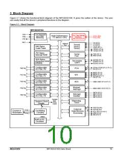
3 Block Diagram
Figure 3-1 shows the functional block diagram of the MPC82G516A. It gives the outline of the device. The user
can easily find all the device’s peripheral functions in the diagram.
Figure 3-1. Block Diagram
MPC82G516A
VDD
VSS
V30
LDO Regulator
and Power
Monitoring
On-Chip Debug
Interface
(for ICE & ICP)
High-Performance
1-T 80C51 CPU
OCD_SDA
OCD_SCL
RST
T0 (P3.4)
T1 (P3.5)
T2 (P1.0)
T2EX (P1.1)
T0CKO (P3.4)
T2CKO (P1.0)
Internal
Bus
Timer0
Timer1
Timer2
64K Bytes
Code Flash
256 Bytes
Internal RAM
TXD (P3.1)
RXD (P3.0)
Serial
Port
1024 Bytes
eXpanded RAM
(XRAM)
S2TXD (P1.3)
S2RXD (P1.2)
S2CKO (P3.5)
Secondary
UART
6
Configurable
I/O Port, P0
CEX0~CEX5 (P1.2~P1.7)
ECI (P1.1)
P0[7:0]
P1[7:0]
P2[7:0]
P3[7:0]
P4[7:0]
PCA
SPI
MISO (P1.6)
MOSI (P1.5)
SPICLK (P1.7)
/SS (P1.4)
Configurable
I/O Port, P1
8
8
Configurable
I/O Port, P2
ADC
AIN0~AIN7 (P1.0~P1.7)
KBI0~KBI7 (P2.0~P2.7)
Configurable
I/O Port, P3
Keypad
Interrupt
/INT0 (P3.2)
/INT1 (P3.3)
/INT2 (P4.3)
/INT3 (P4.2)
Configurable
I/O Port, P4
Interrupt
Handler
System
and
Watchdog
Timer
System Clock
Divider
CPU
Clock
8
8
AD[7:0] (P0)
A[15:8] (P2)
External
Data Memory
Accessing
XTAL1
XTAL2
Crystal or
Resonator
Oscillating
Circuitry
ALE (P3.5 or P4.1)
/WR (P3.6)
/RD (P3.7)
~6MHz
Built-in RC
Oscillator
MEGAWIN
MPC82G516A Data Sheet
10

 MEGAWIN [ MEGAWIN TECHNOLOGY CO., LTD ]