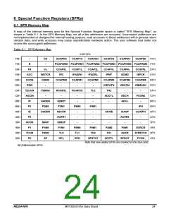
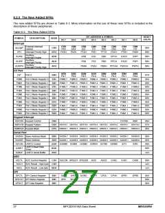
6.2 SFR Introduction
6.2.1 The Standard 80C51 SFRs
The standard 80C51 SFRs are shown in Table 6-2. Among them, the functions of the C51 core registers are
outlined below. More information on the use of the other standard SFRs is included in the description of those
peripherals.
C51 Core Registers
Accumulator: ACC is the Accumulator register. The mnemonics for Accumulator-Specific instructions, however,
refer to the Accumulator simply as A.
B Register: The B register is used during multiply and divide operations. For other instructions it can be treated
as another scratch pad or general purpose register.
Stack Pointer: The Stack Pointer register is 8 bits wide. It denotes the top of the Stack, which is the last used
value. The user can place the Stack anywhere in the internal scratchpad RAM by setting the Stack Pointer to the
desired location, although the lower bytes are normally used for working registers. On reset, the Stack Pointer is
initialized to 07H. This causes the stack to begin at location 08H.
Data Pointer: The Data Pointer (DPTR) consists of a high byte (DPH) and a low byte (DPL). Its intended function
is to hold a 16-bit address to assign a memory address for the MOVX instructions. This address can point to a
program/data memory location, either on- or off-chip, or a memory-mapped peripheral. It may be manipulated as
a 16-bit register or as two independent 8-bit registers.
Program Status Word: The PSW register contains program status information as detailed in the following.
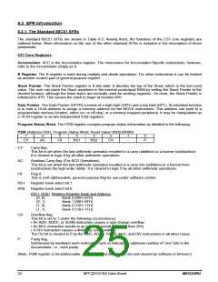
PSW (Address=D0H, Program Status Word, Reset Value=0000,0000B)
7
6
5
4
3
2
1
0
CY
AC
F0
RS1
RS2
OV
-
P
CY:
Carry flag.
This bit is set when the last arithmetic operation resulted in a carry (addition) or a borrow (subtraction).
It is cleared to logic 0 by all other arithmetic operations.
AC:
F0:
Auxiliary Carry flag. (For BCD Operations)
This bit is set when the last arithmetic operation resulted in a carry into (addition) or a borrow from
(subtraction) the high order nibble. It is cleared to logic 0 by all other arithmetic operations.
Flag 0.
This is a bit-addressable, general purpose flag for use under software control.
RS1: Register bank select bit 1.
RS0: Register bank select bit 0.
(RS1, RS0) Working Register Bank and Address
(0, 0)
(0, 1)
(1, 0)
(1, 1)
Bank 0 (00H~07H)
Bank 1 (08H~0FH)
Bank 2 (10H~17H)
Bank 3 (18H~1FH)
OV:
P:
Overflow flag.
This bit is set to 1 under the following circumstances:
• An ADD, ADDC, or SUBB instruction causes a sign-change overflow.
• An MUL instruction results in an overflow (result is greater than 255).
• A DIV instruction causes a divide-by-zero condition.
The OV bit is cleared to 0 by the ADD, ADDC, SUBB, MUL, and DIV instructions in all other cases.
Parity flag.
Set/cleared by hardware each instruction cycle to indicate an odd/even number of “one” bits in the
Accumulator, i.e., even parity.
(Note: PSW register is bit-addressable. All the released bits can be set and cleared by software in bit-level.)
25
MPC82G516A Data Sheet
MEGAWIN

 MEGAWIN [ MEGAWIN TECHNOLOGY CO., LTD ]