MX29LV800T/B
bedded Program Algorithm are ignored. Note that a
hardware reset immediately terminates the programming
operat ion.The Byte Program command sequence should
be reinitiated once the device has reset to reading array
data, to ensure data integrity.
this, the device outputs the "complement,” or "0".” The
system must provide an address within any of the sec-
tors selected for erasure to read valid status information
on Q7.
After an erase command sequence is written, if all sec-
tors selected for erasing are protected, Data Polling on
Q7 is active for approximately 100 us, then the device
returns to reading array data. If not all selected sectors
are protected, the Automatic Erase algorithm erases the
unprotected sectors, and ignores the selected sectors
that are protected.
Programming is allowed in any sequence and across
sector boundaries. A bit cannot be programmed from a
"0" back to a "1". Attempting to do so may halt the
operation and set Q5 to "1" ,” or cause the Data Polling
algorithm to indicate the operation was successful.
However, a succeeding read will show that the data is
still "0". Only erase operations can convert a "0" to a
"1".
When the system detects Q7 has changed from the
complement to true data, it can read valid data at Q7-Q0
on the following read cycles. This is because Q7 may
change asynchr onously with Q0-Q6 while Output En-
able (OE) is asserted low.
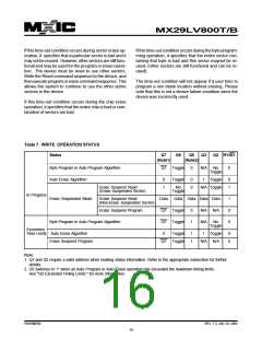
WRITE OPERSTION STATUS
The device provides several bits to determine the sta-
tus of a write operation: Q2, Q3, Q5, Q6, Q7, and RY/
BY.Table 10 and the following subsections describe the
functions of these bits. Q7, RY/BY, and DQ6 each offer
a method for determining whether a program or erase
operation is complete or in progress. These three bits
are discussed first.
RY/BY:Ready/Busy
The RY/BY is a dedicated, open-drain output pin that
indicates whether an Automatic Erase/Program algorithm
is in progress or complete. The RY/BY status is valid
after the rising edge of the final WE or CE, whichever
happens first, in the command sequence. Since RY/BY
is an open-drain output, several RY/BY pins can be tied
together in parallel with a pull-up resistor to Vcc.
Q7: Data Polling
The Data Polling bit, Q7, indicates to the host sys-tem
whether an Automatic Algorithm is in progress or com-
pleted, or whether the device is in Erase Suspend. Data
Polling is valid after the rising edge of the finalWE pulse
in the program or erase command sequence.
If the output is low (Busy), the device is actively erasing
or programming. (This includes programming in the Erase
Suspend mode.)If the output is high (Ready), the device
is ready to read array data (including during the Erase
Suspend mode), or is in the standby mode.
During the Automatic Program algorithm, the device out-
puts on Q7 the complement of the datum programmed
to Q7.This Q7 status also applies to programming dur-
ing Er ase Suspend.When the Automatic Program algo-
rithm is complete, the device outputs the datum pro-
grammed to Q7.The system must provide the program
address to read valid status information on Q7. If a pro-
gram address falls within a protected sector, Data Poll-
ing on Q7 is active for approximately 1 us, then the de-
vice returns to reading array data.
Table 7 shows the outputs for RY/BY during write opera-
tion.
Q6:Toggle BIT I
Toggle Bit I on Q6 indicates whether an Automatic Pro-
gram or Erase algorithm is in progress or complete, or
whether the device has entered the Erase Suspend mode.
Toggle Bit I may be read at any address, and is valid
after the rising edge of the final WE or CE, whichever
happens first, in the command sequence(prior to the pro-
gram or erase operation), and during the sector time-
During the Automatic Erase algorithm, Data Polling pro-
duces a "0" on Q7. When the Automatic Erase algo-
rithm is complete, or if the device enters the Erase Sus-
pend mode, Data Polling produces a "1" on Q7. This is
analogous to the complement/true datum out-put de-
scribed for the Automatic Program algorithm: the erase
function changes all the bits in a sector to "1" prior to
P/N:PM0709
REV. 1.3, JAN. 24, 2002
14

 Macronix [ MACRONIX INTERNATIONAL ]