MX29LA129M H/L
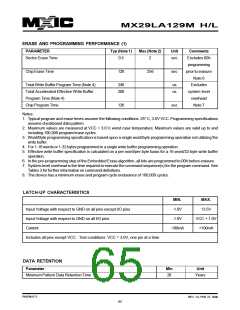
ERASE AND PROGRAMMING PERFORMANCE (1)
PARAMETER
Typ (Note 1)
Max (Note 2)
Unit
Comments
Excludes 00h
programming
prior to erasure
Note 6
Sector Erase Time
0.5
2
sec
Chip Erase Time
128
256
sec
Total Write Buffer Program Time (Note 4)
Total Accelerated Effective Write Buffer
Program Time (Note 4)
240
200
us
us
Excludes
system level
overhead
Chip Program Time
126
sec
Note 7
Notes:
1. Typical program and erase times assume the following conditions: 25° C, 3.0V VCC. Programming specifications
assume checkboard data pattern.
2. Maximum values are measured at VCC = 3.0 V, worst case temperature. Maximum values are valid up to and
including 100,000 program/erase cycles.
3. Word/Byte programming specification is based upon a single word/byte programming operation not utilizing the
write buffer.
4. For 1-16 words or 1-32 bytes programmed in a single write buffer programming operation.
5. Effective write buffer specification is calculated on a per-word/per-byte basis for a 16-word/32-byte write buffer
operation.
6. In the pre-programming step of the Embedded Erase algorithm, all bits are programmed to 00h before erasure.
7. System-level overhead is the time required to execute the command sequence(s) for the program command. See
Tables 3 for further information on command definitions.
8. The device has a minimum erase and program cycle endurance of 100,000 cycles.
LATCH-UP CHARACTERISTICS
MIN.
-1.0V
MAX.
13.5V
Input Voltage with respect to GND on all pins except I/O pins
Input Voltage with respect to GND on all I/O pins
Current
-1.0V
VCC + 1.0V
+100mA
-100mA
Includes all pins except VCC. Test conditions: VCC = 3.0V, one pin at a time.
DATA RETENTION
Parameter
Min
20
Unit
Minimum Pattern Data Retention Time
Years
P/N:PM1171
REV. 1.0, FEB. 27, 2006
65

 Macronix [ MACRONIX INTERNATIONAL ]