MX26C1000B
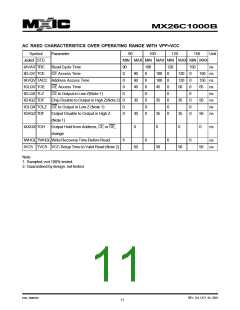
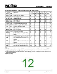
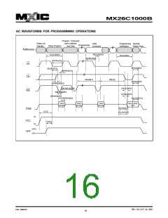
AC CHARACTERISTICS - WRITE/ERASE/PROGRAM OPERATIONS
Symbol
JEDED
Parameter
90
100
120
150
Unit
STD
MIN MAX MIN MAX MIN MAX MIN MAX
tAVAV
tAVWL
tWLAX
tDVWH
tWHDX
tWHGL
tGHWL
tELWL
TWC Write Cycle Time (Note 3)
TAS Address Setup Time
90
0
100
0
120
0
150
0
ns
ns
ns
ns
ns
us
us
ns
ns
ns
ns
us
TAH Address Hold Time
40
40
10
6
40
40
10
6
40
40
10
6
40
40
10
6
TDS Data Setup Time
TDH Data Hold Time
TWR Write Recovery Time Before Read
TDES Read Recovery Time Before Write
0
0
0
0
tCS
tCH
tWP
CE Setup Time Before Write
CE Hold Time
0
0
0
0
tWHEH
tWLWH
tWHWL
tWHWH1
0
0
0
0
Write Pulse Width
50
20
10
50
20
10
50
20
10
50
20
10
tWPH Write Pulse Width High
DurationofProgrammingOperation
(Note2)
tWHWH2
tVPEL
DurationofEraseOperation(Note2)
VPP Setup Time to Chip Enable Low
(Note3)
100
1
100
1
100
1
100
1
ms
us
tVCS
VCC Setup Time to Chip Enable Low
(Note3)
50
50
50
50
us
tVPPR
tVPPF
VPP Rise Time (Note 3) 90% VPPH
VPP Fall Time (Note 3) 10% VPPH
500
500
500
500
500
500
500
500
ns
ns
Note:
1. Read timing characteristics during read/write operations are the same as during read-only operations. Refer to
AC Characteristics for Read Only Operations.
2. Maximum pulse widths not required because the on-chip program/erase circuitry will terminate the pulse widths
internally on the device.
3. Not 100% tested.
REV. 0.6, OCT. 04, 2001
P/N: PM0767
12

 Macronix [ MACRONIX INTERNATIONAL ]