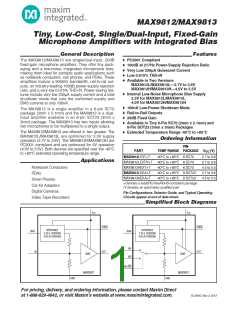
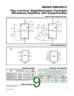
MAX9812/MAX9813
Tiny, Low-Cost, Single/Dual-Input, Fixed-Gain
Microphone Amplifiers with Integrated Bias
ABSOLUTE MAXIMUM RATINGS
(All voltages referenced to GND.)
Operating Temperature Range ...........................-40°C to +85°C
Storage Temperature Range.............................-65°C to +150°C
Junction Temperature......................................................+150°C
Lead Temperature (soldering, 10s) .................................+300°C
Soldering Temperature (reflow) .......................................+260°C
V
........................................................................-0.3V to +6.0V
CC
All Other Pins..............................................-0.3V to (V
+ 0.3V)
CC
Continuous Current (IN, SHDN, IN1, IN2, IN1/IN2)........... 20mA
OUT, BIAS Short-Circuit Duration (to GND or V ) ...Continuous
CC
Continuous Power Dissipation (T = +70°C)
A
SC70 (derate 3.1mW/°C above +70°C).......................245mW
SOT23 (derate 8.9mw/°C above +70°C) .....................714mW
Stresses beyond those listed under “Absolute Maximum Ratings” may cause permanent damage to the device. These are stress ratings only, and functional
operation of the device at these or any other conditions beyond those indicated in the operational sections of the specifications is not implied. Exposure to
absolute maximum rating conditions for extended periods may affect device reliability.
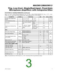
ELECTRICAL CHARACTERISTICS
(V
= 3.3V, I
= 500µA (MAX9812L/MAX9813L), V
= 5V, I
= 800µA (MAX9812H/MAX9813H), V
= 0V, R = open,
GND
L
CC
BIAS
CC
BIAS
SHDN = V , T = T
to T
, unless otherwise noted. Typical values are at T = +25°C.) (Note 1)
MAX A
CC
A
MIN
PARAMETER
GENERAL
SYMBOL
CONDITIONS
MIN
TYP
MAX
UNITS
MAX9812L/MAX9813L
MAX9812H/MAX9813H
= 0A
2.7
4.5
3.6
5.5
400
1
Inferred from
PSRR test
Supply Voltage Range
V
V
CC
Supply Current
I
I
230
0.1
1.5
2.5
85
µA
µA
CC
BIAS
Shutdown Supply Current
I
SHDN = GND
CC_SHDN
MAX9812L/MAX9813L
MAX9812H/MAX9813H
1.35
2.25
1.65
2.75
Amplifier Output Bias Voltage
V
V
OUT_DC
Input Resistance
Voltage Gain
R
kΩ
IN
A
19
90
20
21
dB
V
DC
100
100
100
90
f = 217Hz
f = 1kHz
f = 10kHz
Power-Supply Rejection Ratio
PSRR
Input referred, T = +25°C
dB
OUT
A
V
0.1
-
-
CC
R = 10kΩ to V /2
L
CC
V
OH
V
-
V
CC
0.1V
CC
Output Voltage Swing
R = 1kΩ to V /2
V
L
CC
0.25V
R = 10kΩ to V /2
0.1
0.1
12
L
CC
V
OL
R = 1kΩ to V /2
0.25
24
L
CC
Output Short-Circuit Current
Small-Signal -3dB Bandwidth
Output Capacitive-Load Stability
Output Impedance
I
Sinking or sourcing
= 10mV
3
mA
kHz
pF
OUT_SC
BW
V
400
50
OUT
P-P
C
No sustained oscillations
f = 1kHz
L
Z
0.5
1
Ω
OUT
Output Slew Rate
SR
V
= 1V step
V/µs
OUT
Maxim Integrated
2

 MAXIM [ MAXIM INTEGRATED PRODUCTS ]