-5 V/-1 2 V/-1 5 V o r Ad ju s t a b le ,
Hig h -Effic ie n c y, Lo w I DC-DC In ve rt e rs
Q
45/MAX76
switch is OFF), the range of input and output voltages is
limited to a 21V absolute maximum differential voltage.
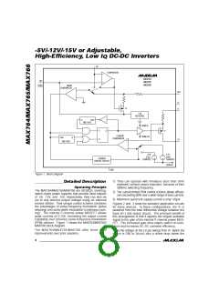
P FM Co n t ro l S c h e m e
The MAX764/MAX765/MAX766 use a proprietary, cur-
rent-limited PFM control scheme that blends the best
features of PFM and PWM devices. It combines the
ultra-low supply currents of traditional pulse-skipping
PFM converters with the high full-load efficiencies of
current-mode pulse-width modulation (PWM) convert-
ers. This control scheme allows the devices to achieve
high efficiencies over a wide range of loads, while the
current-sense function and high operating frequency
allow the use of miniature external components.
When output voltages more negative than -16V are
required, substitute the MAX764/MAX765/MAX766 with
Maxim’s MAX774/MAX775/MAX776 or MAX1774, which
use an external switch.
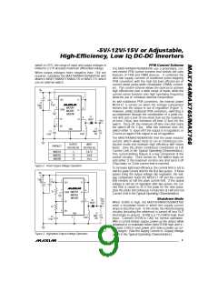
V
IN
7
1
3
V+
OUT
As with traditional PFM converters, the internal power
MOSFET is turned on when the voltage comparator
senses that the output is out of regulation (Figure 1).
However, unlike traditional PFM converters, switching is
accomplished through the combination of a peak cur-
rent limit and a pair of one-shots that set the maximum
on-time (16µs) and minimum off-time (2.3µs) for the
switch. Once off, the minimum off-time one-shot holds
the switch off for 2.3µs. After this minimum time, the
switch either 1) stays off if the output is in regulation, or
2) turns on again if the output is out of regulation.
C2
0.1µF
C1
120µF
20V
MAX764
MAX765
MAX766
6
8
SHDN
V+
LX
2
4
D1
FB
1N5817
V
OUT
REF
C4
68µF
20V
GND
5
L1
47µH
C3
0.1µF
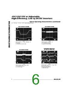
The MAX764/MAX765/MAX766 limit the peak inductor
current, which allows them to run in continuous-con-
duction mode and maintain high efficiency with heavy
loads. (See the photo Continuous Conduction at Full
Current Limit in the Typical Operating Characteristics.)
This current-limiting feature is a key component of the
control circuitry. Once turned on, the switch stays on
until either 1) the maximum on-time one shot turns it off
(16µs later), or 2) the current limit is reached.
OUTPUT
VOLTAGE (V)
INPUT
VOLTAGE (V)
PRODUCT
MAX764
MAX765
MAX766
-5
3 to 15
3 to 8
3 to 5
-12
-15
Figure 2. Fixed Output Voltage Operation
To increase light-load efficiency, the current limit is set to
half the peak current limit for the first two pulses. If those
pulses bring the output voltage into regulation, the volt-
age comparator holds the MOSFET off and the current
limit remains at half the peak current limit. If the output
voltage is still out of regulation after two pulses, the cur-
rent limit is raised to its 0.75A peak for the next pulse.
(See the photo Discontinuous Conduction at Half and Full
Current Limit in the Typical Operating Characteristics.)
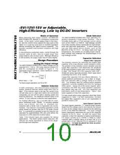
V
IN
C1
C2
0.1µF
120µF
20V
7
6
1
3
2
V+
OUT
SHDN
FB
R2
MAX764
MAX765
MAX766
V+
LX
V
-1V to
-16V
OUT
S h u t d o w n Mo d e
When SHDN is high, the MAX764/MAX765/MAX766
enter a shutdown mode in which the supply current
drops to less than 5µA. In this mode, the internal biasing
circuitry (including the reference) is turned off and OUT
discharges to ground. SHDN is a TTL/CMOS-logic level
input. Connect SHDN to GND for normal operation.
With a current-limited supply, power-up the device while
unloaded or in shutdown mode (hold SHDN high until V+
exceeds 3.0V) to save power and reduce power-up cur-
rent surges. (See the Supply Current vs. Supply Voltage
graph in the Typical Operating Characteristics.)
8
D1
1N5817
R1
C3
4
REF
C4
GND
5
L1
47µH
68µF
20V
0.1µF
Figure 3. Adjustable Output Voltage Operation
_______________________________________________________________________________________
9

 MAXIM [ MAXIM INTEGRATED PRODUCTS ]