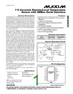
1°C Accurate Remote/Local Temperature
Sensor with SMBus Serial Interface
ABSOLUTE MAXIMUM RATINGS
(All voltages are referenced to GND unless otherwise noted.)
Continuous Power Dissipation (T = +701C)
A
V
..........................................................................-0.3V to +6V
16-Pin QSOP (derate 8.30mW/1C above +701C).........667mW
Operating Temperature Range ........................-551C to +1251C
Junction Temperature......................................................+1501C
Storage Temperature Range ............................-651C to +1651C
Lead Temperature (soldering, 10s) .................................+3001C
CC
DXP, ADD_ ................................................-0.3V to (VCC + 0.3V)
DXN ......................................................................-0.3V to +0.8V
SMBCLK, SMBDATA, ALERT, STBY.. ......................-0.3V to +6V
SMBDATA, ALERT Current .................................-1mA to +50mA
DXN Current ...................................................................... 1mA
ESD Protection (all pins, Human Body Model). .................2000V
Stresses beyond those listed under “Absolute Maximum Ratings” may cause permanent damage to the device. These are stress ratings only, and functional
operation of the device at these or any other conditions beyond those indicated in the operational sections of the specifications is not implied. Exposure to
absolute maximum rating conditions for extended periods may affect device reliability.
ELECTRICAL CHARACTERISTICS
(V
= +3V to +5.5V, T = -551C to +1251C, unless otherwise noted. Typical values are at V
= +3.3V and T = +251C.)
CC A
CC
A
PARAMETER
SYMBOL
CONDITIONS
MIN
TYP
MAX
UNITS
°C
TEMPERATURE-TO-DIGITAL CONVERTER
+60°C ≤ T ≤ +100°C, V
= +3.3V
CC
-1.3
-2
+1.3
+2
A
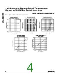
Accuracy (Local Sensor)
0°C ≤ T ≤ +100°C, V
= +3.3V
CC
A
-55°C ≤ T ≤ +120°C, V
= +3.3V
CC
-5
+5
A
+70°C ≤ T ≤ +100°C, V = +3.3V (Note 1)
-1
+1
RJ
CC
Accuracy (Remote Sensor)
0°C ≤ T ≤ +100°C, V
= +3.3V (Note 1)
CC
-2
+2
°C
RJ
-55°C ≤ T ≤ +120°C, V = +3.3V (Notes 1, 2)
-5
+5
RJ
CC
Line Regulation
0.2
+8
0.5
°C
°C
+1
Resolution (Legacy Mode)
Conversion rate >1Hz
Bits
°C
+0.125
Resolution (Extended Mode)
Conversion rate ≤1Hz
+11
Bits
Undervoltage Lockout
UVLO
V
input, disables A/D conversion,
CC
+2.60
+2.80
+2.95
V
Threshold
rising edge
Undervoltage Lockout
Hysteresis
+90
mV
Supply Voltage Range
Power-On Reset (POR) Threshold
POR Threshold Hysteresis
Standby Current
V
+3.0
+1.5
+5.5
+2.5
V
CC
V
, falling edge
+2.0
+90
V
CC
mV
µA
mA
SMBus static
+3
+10
+1
Operating Current
During conversion
+0.55
+40
0.25 conversion/s (Note 3)
2 conversion/s (Note 3)
+70
+250
Average Operating Current
µA
+150
From stop bit to conversion completed, in
legacy mode (Note 3)
Conversion Time
t
+95
+125
+156
ms
%
CONV
Conversion Timing Error
Remote Diode Current
25
+120
+12
High level
Low level
+80
+8
+100
+10
I
µA
RJ
2
_______________________________________________________________________________________

 MAXIM [ MAXIM INTEGRATED PRODUCTS ]