65V, Low-Quiescent-Current, High-Voltage Linear
Regulators with µP Reset and Watchdog Timer
ABSOLUTE MAXIMUM RATINGS
IN to GND................................................................-60V to +70V
Thermal Resistance:
EN to GND...................................................-0.3V to (V + 0.3V)
(θ ) .............................................................................52°C/W
JC
IN
JA
HOLD to GND...........................................-0.3V to (V
+ 0.3V)
(θ ) ...............................................................................2°C/W
OUT
SET, WDI, OUT to GND.......................................-0.3V to +13.2V
RESET to GND (Open Drain)...............................-0.3V to +13.2V
Short-Circuit Duration.................................................Continuous
Maximum Current to Any Pin (Except IN, OUT)............... 20mA
Operating Temperature Range .........................-40°C to +125°C
Junction Temperature......................................................+150°C
Storage Temperature Range.............................-65°C to +150°C
Lead Temperature (soldering, 10s) .................................+300°C
Continuous Power Dissipation (T = +70°C)
A
8-Pin SO (derate 19.2mW/°C above +70°C)..............1538mW
Stresses beyond those listed under “Absolute Maximum Ratings” may cause permanent damage to the device. These are stress ratings only, and functional
operation of the device at these or any other conditions beyond those indicated in the operational sections of the specifications is not implied. Exposure to
absolute maximum rating conditions for extended periods may affect device reliability.
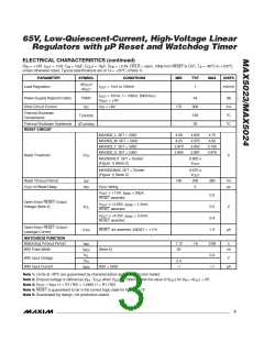
ELECTRICAL CHARACTERISTICS
(V = +14V, I
= 1mA, C = 10µF, C
= 15µF, V = +2.4V, HOLD = open, 10kΩ from RESET to OUT, T = -40°C to +125°C,
IN
OUT
IN
OUT EN A
unless otherwise noted. Typical specifications are at T = +25°C.) (Note 1)
A
PARAMETER
Input Voltage Range
Reverse Input Current
SYMBOL
CONDITIONS
must be at least 1.5V greater than V
= -60V
MIN
TYP
MAX
65
UNITS
V
V
V
V
6.5
IN
REVERSE
IN
IN
OUT
I
0.1
58
10
µA
I
= 0mA
140
OUT
Supply Current
I
Measured at GND
µA
µA
Q
I
= 150mA
2000
6
OUT
Shutdown Supply Current
REGULATOR
I
V
≤ +0.4V
16
SHDN
EN
Guaranteed Output Current
I
V
= +5V
150
4.8
mA
V
OUT
OUT
SET = GND, I
5V version
= 1mA to 150mA,
= 1mA to 150mA,
OUT
5
5.2
Output Voltage
V
OUT
SET = GND, I
3.3V version
OUT
3.168
2.5
3.3
3.432
I
I
= 5mA, adjustable version (MAX5024)
11
OUT
Dropout Voltage
∆V
= 150mA, V = +5V (Note 2)
OUT
0.9
1.5
V
DO
LOAD
Rising edge of V to V
IN
SET = GND
, R = 500Ω,
L
OUT
Startup Response Time
400
µs
+5V version
-1
1
∆V
∆V
/
OUT
Line Regulation
Enable Voltage
+8V ≤ V ≤ +65V
mV/V
V
IN
+3.3V version
-0.5
2.4
0.5
IN
EN = high, regulator on
EN = low, regulator off
V
EN
0.4
0.4
V
V
= +2.4V
= +14V
0.5
4
EN
EN
Enable Input Current
HOLD Voltage
I
µA
V
EN
V
Regulator on, EN transition from high to low
IL
V
0.4V
-
OUT
HOLD Release Voltage
V
EN = low, regulator shuts off
V
IH
HOLD Pullup Current
I
Internally connected to OUT
4
µA
V
HOLD
SET Reference Voltage
SET Input Leakage Current
V
I
= 10mA
OUT
1.223
1.248
0.5
1.273
100
SET
I
nA
SET
2
_______________________________________________________________________________________

 MAXIM [ MAXIM INTEGRATED PRODUCTS ]