High-Speed, Low-Voltage, CMOS Analog
Multiplexers/Switches
78/MAX4619
The logic-level thresholds are TTL/CMOS compatible
when V is +5V. As V rises, the threshold increas-
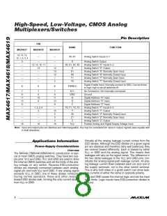
Pin Nomenclature
The MAX4617/MAX4618/MAX4619 are pin compatible
with the industry-standard 74HC4051/74HC4052/
74HC4053 and the MAX4581/MAX4582/MAX4583. In
single-supply applications, they function identically and
have identical logic diagrams, although these parts dif-
fer electrically.
CC
es; as V
CC
falls, the threshold decreases. For example,
= +3V the guaranteed minimum logic-high
CC
CC
when V
threshold decreases to 2.0V
Power Supply
These devices operate from a single supply between
+2.5V and +5.5V. All of the bipolar precautions must be
observed. At room temperature, they actually “work”
with a single supply near or below +2V, although as
supply voltage decreases, switch on-resistance
becomes very high.
The pin designations and logic diagrams in this data
sheet conform to the original 1972 specifications pub-
lished by RCA for the CD4051/CD4052/CD4053. These
designations differ from the standard Maxim switch and
mux designations found on other Maxim data sheets
(including the MAX4051/MAX4052/MAX4053) and may
cause confusion. Designers who feel more comfortable
with Maxim’s standard designations are advised that
the pin designations and logic diagrams on the
MAX4051/MAX4052/MAX4053 data sheet may be freely
applied to the MAX4617/MAX4618/MAX4619.
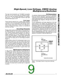
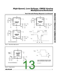
Overvoltage Protection
Proper power-supply sequencing is recommended for
all CMOS devices. Do not exceed the absolute maxi-
mum ratings because stresses beyond the listed rat-
ings can cause permanent damage to the devices.
Always sequence V
on first, followed by the logic
CC
inputs and analog signals. If power-supply sequencing
is not possible, add two small signal diodes (D1, D2) in
series with the supply pins for overvoltage protection
(Figure 1).
V
CC
D1
EXTERNAL
BLOCKING DIODE
Adding diodes reduces the analog-signal range to one
diode drop below V
and one diode drop above
CC
MAX4617
MAX4618
MAX4619
GND, but does not affect the devices’ low switch resis-
tance and low leakage characteristics. Device opera-
V
V
CC
tion is unchanged, and the difference between V
CC
*
*
*
and GND should not exceed 6V. These protection
diodes are not recommended if signal levels must
extend to ground.
X, Y, Z
X_, Y_, Z_
*
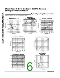
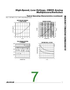
High-Frequency Performance
In 50Ω systems, signal response is reasonably flat up
to 50MHz (see Typical Operating Characteristics).
Above 20MHz, the on-response has several minor
peaks that are highly layout dependent. The problem is
not turning the switch on, but turning it off. The off-state
switch acts like a capacitor and passes higher frequen-
cies with less attenuation. At 10MHz, off-isolation is
about -50dB in 50Ω systems, becoming worse (approx-
imately 20dB per decade) as frequency increases.
Higher circuit impedances also degrade off-isolation.
Adjacent channel attenuation is about 3dB above that
of a bare IC socket and is entirely due to capacitive
coupling.
EE
D2
EXTERNAL
BLOCKING DIODE
GND
*INTERNAL PROTECTION DIODES
Figure 1. Overvoltage Protection Using External Blocking
Diodes
_______________________________________________________________________________________
9

 MAXIM [ MAXIM INTEGRATED PRODUCTS ]