SOT23, 3V/5V, Single-Supply, Rail-to-Rail
Instrumentation Amplifiers
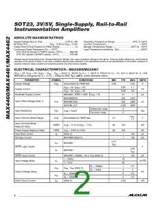
ABSOLUTꢂ MAXIMUM RATINꢁS
Supply Voltage (V
to V ) ...................................-0.3V to +6V
Operating Temperature Range ...........................-40°C to +85°C
Junction Temperature......................................................+150°C
Storage Temperature Range.............................-65°C to +150°C
Lead Temperature (soldering, 10s)....................................300°C
DD
SS
All Other Pins ...................................(V - 0.3V) to (V
+ 0.3V)
SS
DD
Output Short-Circuit Duration to Either Supply.........................1s
Continuous Power Dissipation (T = +70°C)
A
6-Pin SOT23 (derate 8.7mW/°C above +70°C)............695mW
8-Pin SO (derate 5.9mW/°C above +70°C)..................470mW
Stresses beyond those listed under “Absolute Maximum Ratings” may cause permanent damage to the device. These are stress ratings only, and functional
operation of the device at these or any other conditions beyond those indicated in the operational sections of the specifications is not implied. Exposure to
absolute maximum rating conditions for extended periods may affect device reliability.
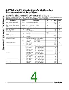
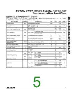
ꢂLꢂCTRICAL CHARACTꢂRISTICS—MAX4460/MAX4461
(V
= 5V, V
= 0V, V
= V
- V
= 50mV to 100mV for G = 1, 20mV to 100mV for G = 10, 2mV to 48mV for G =100,
IN-
DD
CM
DIFF
IN+
MAX4460 is configured for G = 10, R = 200kΩ to GND, T = +25°C, unless otherwise noted.)
L
A
PARAMETER
Supply Voltage
SYMBOL
CONDITIONS
Guaranteed by PSRR test
MIN
TYP
MAX
5.25
1.1
UNITS
V
2.85
V
DD
V
V
= 5V, V
= 3V, V
= 0V
= 0V
0.80
0.68
0.1
50
DD
DD
DIFF
DIFF
Supply Current
mA
µA
0.9
Shutdown Supply Current
MAX4461, SHDN = GND
MAX4460ESA
V
= 5V
1
DD
425
300
600
Input Offset Voltage (Note 1)
V
µV
MAX4461ESA
50
OS
MAX446_EUT
100
2
Differential mode
Common mode
Input Resistance
R
V
= V /2
GΩ
V
IN
CM
DD
2
V
-
DD
Input Common-Mode Range
V
Guaranteed by CMRR test
-0.1
CM
1.7
Input Common-Mode
Rejection Ratio
CMRR
PSRR
V
V
= -0.1V to (V
- 1.7V)
90
80
120
dB
CM
DD
DD
Power-Supply Rejection Ratio
Input Bias Current
= 2.85V to 5.25V
100
1
dB
pA
pA
I
(Note 2)
100
100
B
FB Input Current
MAX4460 (Note 2)
1
0.7 X
V
DD
V
MAX4461
MAX4461
IH
SHDN Logic Levels
V
0.3 X
V
IL
V
DD
SHDN Input Current
MAX4461, V
f = 10kHz
f = 1kHz
= 0V or V (Note 2)
1
18
38
1
100
pA
SHDN
DD
Input Voltage Noise
e
nV/√Hz
n
R = 200kΩ
L
2.5
5
V
V
- V
OH
(Note 3)
OH
DD
R = 20kΩ
L
3
Output Voltage Swing
Short-Circuit Current
mV
mA
R = 200kΩ
L
0
0.2
0.2
V
OL
R = 20kΩ
L
0
I
(Note 4)
150
SC
2
_______________________________________________________________________________________

 MAXIM [ MAXIM INTEGRATED PRODUCTS ]