MAX44246
36V, Low-Noise, Precision, Dual Op Amp
ABSOLUTE MAXIMUM RATINGS
Supply Voltage (V
to GND) .............................-ꢂ.3V to +4ꢂV
Continuous Power Dissipation (T = +7ꢂNC)
DD
A
All Other Pins................................(GND - ꢂ.3V) to (V
Short-Circuit Duration, OUTA,
OUTB to Either Supply Rail………………………… ............. 1s
Continuous Input Current (Any Pin) ..................................2ꢂmA
Differential Input Current................................................. Q2ꢂmA
Differential Input Voltage (Note 1)....................................... .Q6V
+ ꢂ.3V)
ꢁ-Pin FMAX (derate 4.ꢁmW/C above +7ꢂNC) .........3ꢁ7.ꢁmW
ꢁ-Pin SO (derate 4.ꢁmW/C above +7ꢂNC)..............47ꢂ.6mW
Operating Temperature Range........................ -4ꢂNC to +12ꢀNC
Junction Temperature ....................................................+1ꢀꢂNC
Storage Temperature Range............................ -6ꢀNC to +1ꢀꢂNC
Lead Temperature (soldering,1ꢂs) .................................+3ꢂꢂNC
Soldering Temperature (reflow) ......................................+26ꢂNC
DD
Note 1: The amplifier inputs are connected by internal back-to-back clamp diodes. In order to minimize noise in the input stage,
current-limiting resistors are not used. If differential input voltages exceeding 1V are applied, limit input current to 2ꢂmA.
Stresses beyond those listed under “Absolute Maximum Ratings” may cause permanent damage to the device. These are stress ratings only, and functional opera-
tion of the device at these or any other conditions beyond those indicated in the operational sections of the specifications is not implied. Exposure to absolute
maximum rating conditions for extended periods may affect device reliability.
PACKAGE THERMAL CHARACTERISTICS (Note 2)
µMAX
SO
Junction-to-Ambient Thermal Resistance (q ) ........12ꢂNC/W
Junction-to-Ambient Thermal Resistance (q ) ........221NC/W
JA
JA
Junction-to-Case Thermal Resistance (q ) ..............42NC/W
Junction-to-Case Thermal Resistance (q ) ..............37NC/W
JC
JC
Note 2: Package thermal resistances were obtained using the method described in JEDEC specification JESDꢀ1-7, using a four-layer
board. For detailed information on package thermal considerations, refer to www.maximintegrated.com/thermal-tutorial.
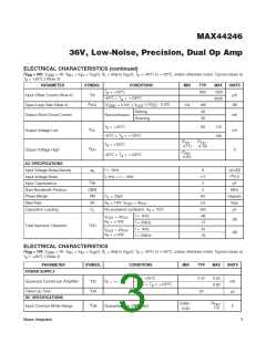
ELECTRICAL CHARACTERISTICS
(V
= 30V, V
= ꢂV, V
= V = V /2, R = ꢀkΩ to V /2, T = -4ꢂ°C to +12ꢀ°C, unless otherwise noted. Typical values at
DD
GND
IN+ IN- DD L DD A
T
= +2ꢀ°C.) (Note 3)
A
PARAMETER
SYMBOL
CONDITIONS
Guaranteed by PSRR
MIN
2.7
TYP
166
ꢂ.42
2ꢂ
MAX
UNITS
V
Supply Voltage Range
DD
36
V
V
V
= 2.7V to 36V, T =
+2ꢀNC
= 2.7V to 36V, -4ꢂNC < T < +12ꢀNC
14ꢁ
146
Power-Supply Rejection Ratio
(Note 4)
DD
A
PSRR
dB
DD
A
T
=
+2ꢀNC
ꢂ.ꢀꢀ
ꢂ.6ꢂ
A
I
Quiescent Current per Amplifier
DD
R = J
mA
L
-4ꢂNC < T
<
+12ꢀNC
A
t
Power-Up Time
ON
Fs
DC SPECIFICATIONS
Input Common-Mode Range
V
CM
Guaranteed by CMRR test
= (V + ꢂ.ꢂꢀV) to (V - 1.ꢀV)
DD
V
- ꢂ.ꢂꢀ
V
- 1.ꢀ
V
GND
146
DD
Common-Mode Rejection Ratio
(Note 4)
CMRR
V
166
1
dB
CM
GND
V
Input Offset Voltage (Note 4)
OS
ꢀ
FV
Input Offset Voltage Drift
(Note 4)
TC V
1
2ꢂ
nV/NC
OS
T
=
+2ꢀNC
3ꢂꢂ
6ꢂꢂ
12ꢀꢂ
A
Input Bias Current (Note 4)
I
pA
B
-4ꢂNC < T
<
+12ꢀNC
A
Maxim Integrated
2

 MAXIM [ MAXIM INTEGRATED PRODUCTS ]