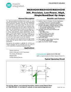
MAX44244/MAX44245/MAX44248
36V, Precision, Low-Power, 90µA,
Single/Quad/Dual Op Amps
ABSOLUTE MAXIMUM RATINGS
V
to V ............................................................-0.3V to +40V
Operating Temperature Range........................ -40NC to +125NC
Storage Temperature ....................................... -65NC to +150NC
Junction Temperature .....................................................+150NC
Lead Temperature (soldering, 10s) ................................+300NC
Soldering Temperature (reflow) ......................................+260NC
DD
SS
Common-Mode Input Voltage........(V - 0.3V) to (V
+ 0.3V)
SS
DD
Differential Input Voltage IN_+, IN_- ......................................6V
Continuous Input Current Into Any Pin ........................... Q20mA
Output Voltage to V (OUT_) ................– 0.3V to (V
+ 0.3V)
SS
DD
Output Short-Circuit Duration (OUT_)..................................... 1s
Stresses beyond those listed under “Absolute Maximum Ratings” may cause permanent damage to the device. These are stress ratings only, and functional opera-
tion of the device at these or any other conditions beyond those indicated in the operational sections of the specifications is not implied. Exposure to absolute
maximum rating conditions for extended periods may affect device reliability.
PACKAGE THERMAL CHARACTERISTICS (Note 1)
SO-8
Junction-to-Ambient Thermal Resistance (B ) ........132NC/W
TSSOP
Junction-to-Ambient Thermal Resistance (B ) ........110NC/W
JA
JA
Junction-to-Case Thermal Resistance (B )...............38NC/W
Junction-to-Case Thermal Resistance (B )...............30NC/W
JC
JC
SO-14
FMAX
Junction-to-Ambient Thermal Resistance (B ) ........120NC/W
Junction-to-Ambient Thermal Resistance (B ) .....206.3NC/W
JA
JA
Junction-to-Case Thermal Resistance (B )...............37NC/W
SOT23
Junction-to-Case Thermal Resistance (B )...............42NC/W
JC
JC
Junction-to-Ambient Thermal Resistance (B ) .....324.3NC/W
JA
Junction-to-Case Thermal Resistance (B )...............82NC/W
JC
Note 1: Package thermal resistances were obtained using the method described in JEDEC specification JESD51-7, using a four-layer
board. For detailed information on package thermal considerations, refer to www.maximintegrated.com/thermal-tutorial.
ELECTRICAL CHARACTERISTICS
(V
= 10V, V = 0V, V
= V = V /2, R = 5kI to V /2, T = -40NC to +125NC, unless otherwise noted. Typical values are
DD
SS
IN+
IN-
DD
L
DD
A
at +25NC.) (Note 2)
PARAMETER
SYMBOL
CONDITIONS
MIN
TYP
MAX
UNITS
POWER SUPPLY
Supply Voltage Range
V
Guaranteed by PSRR
= +25NC, V = V = V /2 - 1V
2.7
140
133
36
V
DD
T
148
100
90
Power-Supply Rejection Ratio
(Note 3)
A
IN+
IN-
DD
PSRR
dB
-40NC < T < +125NC
A
T
= +25NC
160
190
130
145
Quiescent Current Per Amplifier
(MAX4244 Only)
A
I
I
FA
FA
DD
DD
-40NC < T < +125NC
A
T
= +25NC
Quiescent Current Per Amplifier
(MAX44245/MAX44248 Only)
A
-40NC < T < +125NC
A
DC SPECIFICATIONS
V
0.05
-
V
1.5
-
SS
DD
Input Common-Mode Range
V
Guaranteed by CMRR test
V
CM
Maxim Integrated
2

 MAXIM [ MAXIM INTEGRATED PRODUCTS ]