MAX44244/MAX44245/MAX44248
36V, Precision, Low-Power, 90µA,
Single/Quad/Dual Op Amps
circuit, both the DAC and the reference are referred to
a high-accuracy internal oscillator that requires no
external components.
the local ground. The MAX44244 op-amp inputs are
capable of swinging to the negative supply (which is the
local ground in this case). R3 acts as a current mirror with
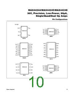
Layout Guidelines
The MAX44244/MAX44245/MAX44248 feature ultra-low
input offset voltage and noise. Therefore, to get optimum
performance follow the layout guidelines.
R
. Therefore, if R
= 50Ω (i.e. 20mA will drop
SENSE
SENSE
1V) and if the current through R3 is 10µA when I
is
OUT
20mA (0.05% error) then R3 = 100kΩ. R1 is chosen along
with the reference voltage to provide the 4mA offset. R2
= 512kΩ for 20mA full scale or R2 = 614kΩ for 20% over-
Avoid temperature tradients at the junction of two
dissimilar metals. The most common dissimilar metals
used on a PCB are solder-to-component lead and
solder-to-board trace. Dissimilar metals create a local
thermocouple. A variation in temperature across the
board can cause an additional offset due to Seebeck
effect at the solder junctions. To minimize the Seebeck
effect, place the amplifier away from potential heat
sources on the board, if possible. Orient the resistors
such that both the ends are heated equally. It is a good
practice to match the input signal path to ensure that the
type and number of thermoelectric juntions remain the
same. For example, consider using dummy 0ω resistors
oriented in such a way that the thermoelectric source, due
to the real resistors in the signal path, are cancelled. It is
recommended to flood the PCB with ground plane. The
ground plane ensures that heat is distributed uniformly
reducing the potential offset voltage degradation due to
Seebeck effect.
range. R
is ratiometric with R3, R1 independently
SENSE
sets the offset current and R2 independently sets the
DAC scaling.
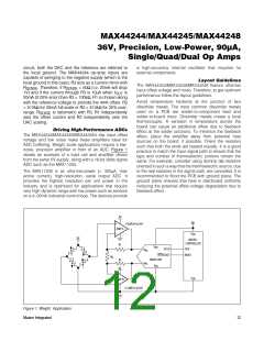
Driving High-Performance ADCs
The MAX44244/MAX44245/MAX44248’s low input offset
voltage and low noise make these amplifiers ideal for
ADC buffering. Weight scale applications require a low-
noise, precision amplifier in front of an ADC. Figure 1
details an example of a load cell and amplifier driven
from the same 5V supply, along with a 16-bit delta sigma
ADC such as the MAX11205.
The MAX11205 is an ultra-low-power (< 300FA, max
active current), high-resolution, serial output ADC. It
provides the highest resolution per unit power in the
industry and is optimized for applications that require
very high dynamic range with low power such as sensors
on a 4–20mA industrial control loop. The devices provide
5V
5V
½ MAX44248
AMP A
V
DD
5V
MICRO-
CONTROLLER
R
R
F
V
DD
SCLK
RDY/DOUT
MAX11205
SCK
V
V
IN+
IN-
MISO
R
G
F
V
SS
5V
V
SS
AMP B
½ MAX44248
Figure 1. Weight Application
Maxim Integrated
12

 MAXIM [ MAXIM INTEGRATED PRODUCTS ]