MAX2560/MAX2566/MAX2572 Evaluation Kits
DCS 1800 Mode
Perform the following steps to evaluate the
MAX2566/MAX2572 in the DCS 1800 mode:
3) Connect the I and Q outputs of the arbitrary wave-
form generator to the I (J15) and Q (J16) ports. Set
the generator to GSM settings. Verify 300mV peak
baseband signal on Q+/Q- (JU2) and I+/I- (JU1), or
600mV peak-to-peak differential.
1) Verify shunts JU23–JU26 and JU33 positions with
Table 4.
4) The MAX2566 EV kit requires an external LO input.
Apply an external LO 1610MHz at -10dBm to the
LOH port.
2) With MAX2560/MAX2566/MAX2572 control software
active in the REG screen, use Tables 2 and 3 to set
the operating mode to DCS 1800 mode.
5) Connect GSM (J33) to the spectrum analyzer.
Configure the spectrum analyzer to measure spec-
tral mask for the GSM signal. Set the center fre-
quency to 1900MHz with a +10dBm reference level.
3) Connect the I and Q outputs of the arbitrary wave-
form generator to the I (J15) and Q (J16) ports. Set
the generator to GSM settings. Verify 300mV peak
baseband signal on Q+/Q- (JU2) and I+/I- (JU1), or
600mV peak-to-peak differential.
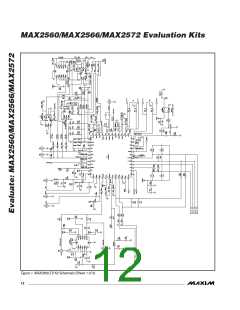
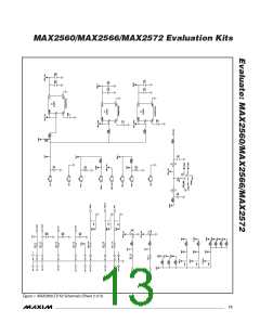
Layout Considerations
4) The MAX2566 EV kit requires an external LO input.
Apply an external LO 1510MHz at -10dBm to the
LOH port.
The MAX2560/MAX2566/MAX2572 EV kits can serve as
guides for board layout. Keep PC board trace lengths
as short as possible to minimize parasitics. Also, keep
decoupling capacitors as close to the IC as possible
with a direct connection to the ground plane.
5) Connect GSM (J33) to the spectrum analyzer.
Configure the spectrum analyzer to measure spec-
tral mask for the GSM signal. Set the center fre-
quency to 1800MHz with 50MHz span and a
+10dBm reference level.
INTF2300 SPI Interface Board
The INTF2300 interface board is used to interface 3-
wire SPI protocol from a PC’s parallel port to the EV kit.
This board level translates 5V logic from the PC to VCC
of the EV kit (typically, this is 2.85V logic). The INTF2300
also provides buffering and EMI filtering. Its absolute
maximum supply voltage is 4.6V, limited by the break-
down of the buffer IC. The recommended operating
supply voltage range is +2.7V to +3.6V.
GSM 1900 Mode
Perform the following steps to evaluate the
MAX2566/MAX2572 in the GSM 1900 mode:
1) Verify shunts JU23–JU26 and JU33 positions with
Table 4.
2) With MAX2560/MAX2566/MAX2572 control software
active in the REG screen, use Tables 2 and 3 to set
the operating mode to GSM 1900 mode.
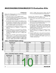
Table 3. MAX2572 Register Settings
REGISTER (hex)
FRAC_SYNTH
FRAC
WCDMA
070778
062763
000302
00D80D
0DF77F
07A103
000000
GSM 900
0B075B
089D8A
000244
00D80D
0D876F
07BD07
000000
DCS 1800
0B0774
027627
000244
00D80D
0D876F
04BD07
000000
GSM 1900
0B077B
0D89D9
000244
IF_N
IF_SYNTH
OPCTRL
CONFIG
TEST
00D80D
0D876F
04BD0F
000000
Table 4. GSM Jumper Settings
JU25
LOW
LOW
HIGH
MODE
JU23
JU24
JU26
JU33
LOW
HIGH
HIGH
GSM 900
DCS 1800
GSM 1900
CLOSE
CLOSE
CLOSE
LOGSM1
LOGSM1
LOGSM1
LOW
HIGH
HIGH
______________________________________________________________________________________ 11

 MAXIM [ MAXIM INTEGRATED PRODUCTS ]