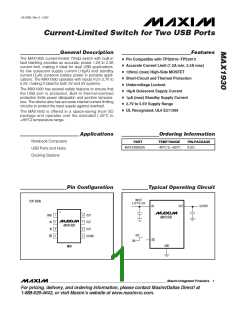
Current-Limited Switch for Two USB Ports
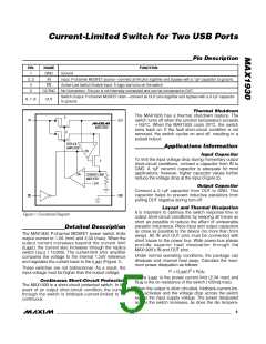
Pin Description
PIN
1
NAME
FUNCTION
GND
IN
Ground
2, 3
4
Input. P-channel MOSFET source—connect all IN pins together and bypass with a 1µF capacitor to ground.
Active-Low Switch Enable Input. A logic low turns on the switch.
EN
5
OUTNC
No Connection. This pin is not internally connected and can be connected to OUT.
Switch Output. P-channel MOSFET drain—connect all OUT pins together and bypass with a 0.1µF capacitor
to ground.
6, 7, 8
OUT
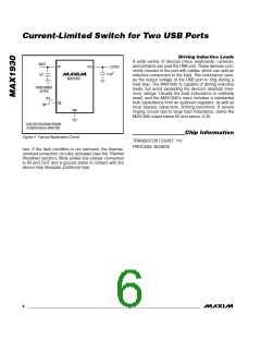
Thermal Shutdown
The MAX1930 has a thermal shutdown feature. The
P
IN
OUT
switch turns off when the junction temperature exceeds
+165°C. When the MAX1930 cools 20°C, the switch
turns back on. If the fault short-circuit condition is not
removed, the switch cycles on and off, resulting in a
pulsed output.
MAX1930
P
REPLICA
AMPLIFIER
Applications Information
ON
Input Capacitor
To limit the input voltage drop during momentary output
short-circuit conditions, connect a capacitor from IN to
GND. A 1µF ceramic capacitor is adequate for most
applications; however, higher capacitor values further
reduce the voltage drop at the input (Figure 2).
P
ON
CURRENT-LIMIT
AMPLIFIER
1.24V
Output Capacitor
Connect a 0.1µF capacitor from OUT to GND. This
capacitor helps to prevent inductive parasitics from
pulling OUT negative during turn-off.
GND
EN
Layout and Thermal Dissipation
It is important to optimize the switch response time to
output short-circuit conditions by keeping all traces as
short as possible to reduce the effect of undesirable
parasitic inductance. Place input and output capacitors
as close as possible to the device (no more than 5mm
away). All IN and OUT pins must be connected with
short traces to the power bus. Wide power-bus planes
provide superior heat dissipation through the
MAX1930’s IN and OUT pins.
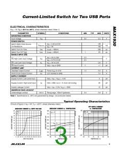
Figure 1. Functional Diagram
Detailed Description
The MAX1930 P-channel MOSFET power switch limits
output current to 1.2A (min) and 2.3A (max). When the
output current increases beyond the current limit
(I
), the current also increases through the replica
LIMIT
switch (I
/ 13,000). The current-limit error amplifier
OUT
Under normal operating conditions, the package can
dissipate and channel heat away. Calculate the maxi-
mum power dissipation as follows:
compares the voltage to the internal 1.24V reference
and regulates the current back to the I (Figure 1).
LIMIT
These switches are not bidirectional. As a result, the
input voltage must be higher than the output voltage.
2
✕
P = (I
)
R
ON
LIMIT
where I
ON
is the preset current limit (2.3A max) and
LIMIT
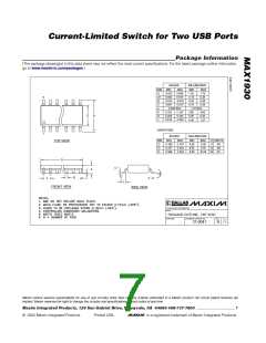
Continuous Short-Circuit Protection
The MAX1930 is a short-circuit protected switch. In the
event of an output short-circuit condition, the current
through the switch is foldback-current-limited to 1A
continuous.
R
is the on-resistance of the switch (125m max).
When the output is short circuited, foldback-current-lim-
iting activates and the voltage drop across the switch
equals the input supply voltage. The power dissipated
across the switch increases, as does the die tempera-
_______________________________________________________________________________________
5

 MAXIM [ MAXIM INTEGRATED PRODUCTS ]