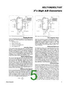
ICL7106/ICL7107
31⁄2 Digit A/D Converters
ABSOLUTE MAXIMUM RATINGS
Supply Voltage
Continuous Power Dissipation (T = +70NC)(Note 2)
A
PDIP (derate 16.7mW/NC above +70NC)................1333.3mW
PLCC (derate 13.3mW/NC above +70NC)...............1066.7mW
Operating Temperature Range............................. 0NC to +70NC
Storage Temperature Range............................ -55NC to +160NC
Lead Temperature (soldering, 10s) ................................+300NC
Soldering Temperature (reflow)
ICL7106, V+ to V-..............................................................15V
ICL7107, V+ to GND ........................................................ +6V
ICL7107, V- to GND ...........................................................-9V
Analog Input Voltage (either input) (Note 1)................. V+ to V-
Reference Input Voltage (either input)...........................V+ to V-
Clock Input
PDIP.............................................................................+260NC
PLCC ...........................................................................+245NC
ICL7106.................................................................TEST to V+
ICL7107................................................................. GND to V+
Note 1: Input voltages may exceed the supply voltages, provided the input current is limited to 100ꢀA.
Note 2: Dissipation rating assumes device is mounted with all leads soldered to the PCB.
Stresses beyond those listed under “Absolute Maximum Ratings” may cause permanent damage to the device. These are stress ratings only, and functional
operation of the device at these or any other conditions beyond those indicated in the operational sections of the specifications is not implied. Exposure to absolute
maximum rating conditions for extended periods may affect device reliability.
ELECTRICAL CHARACTERISTICS
(Note 3)
PARAMETER
Zero Input Reading
CONDITIONS
MIN
TYP
MAX
UNITS
Digital
Reading
V
V
= 0V, full scale = 200.0mV
-000.0 000.0 +000.0
999 999/1000 1000
IN
Digital
Reading
Ratiometric Reading
= V
, V
= 100mV
IN
REF REF
Rollover Error (Difference in Reading for
Equal Positive and Negative Reading Near -V = +V = 200.0mV
Full Scale)
-1
-1
Q2
+1
+1
Counts
IN
IN
Linearity (Maximum Deviation from Best
Straight Line Fit)
Full scale = 200mV or full scale = 2.000V
Q2
50
15
Counts
FV/V
FV
Common-Mode Rejection Ratio (Note 4)
V = Q1V, V = 0V, full scale = 200.0mV
CM IN
Noise (Pk-Pk Value Not Exceeded
95% of Time)
V
= 0V, full scale = 200mV
= 0V
IN
Input Leakage Current
Zero Reading Drift
V
V
V
1
10
1
pA
IN
IN
IN
= 0V, 0NC < T < +70NC
0.2
FV/NC
A
= 199.0mV, 0NC < T < +70NC
A
Scale Factor Temperature Coefficient
1
5
ppm/NC
(external reference 0ppm/NC)
V+ Supply Current (Does Not Include LED
Current for ICL7107)
V
= 0V
0.8
0.6
2.8
1.8
1.8
3.2
mA
mA
V
IN
V- Supply Current (ICL7107 Only)
Analog Common Voltage
(With Respect to Positive Supply)
25kI between common and positive supply
25kI between common and positive supply
2.4
Temperature Coefficient of Analog
Common (With Respect to Positive Supply)
80
ppm/NC
The electrical characteristics above are a reproduction of a portion of Intersil's copyrighted (1983/1984) data book. This information
does not constitute any representation by Maxim that Intersil's products will perform in accordance with these specifications. The
"Electrical Characteristics table" along with the descriptive excerpts from the original manufacturer's data sheet have been included
in this data sheet solely for comparative purposes.
2
Maxim Integrated

 MAXIM [ MAXIM INTEGRATED PRODUCTS ]