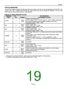
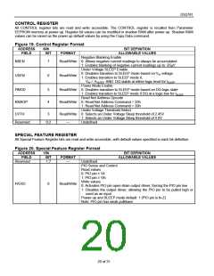
DS2781
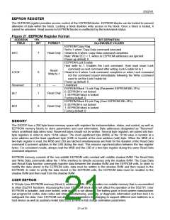
EEPROM REGISTER
The EEPROM register provides access control of the EEPROM blocks. EEPROM blocks can be locked to prevent
alteration of data within the block. Locking a block disables write access to the block. Once a block is locked, it
cannot be unlocked. Read access to EEPROM blocks is unaffected by the lock/unlock status.
Figure 21. EEPROM Register Format
ADDRESS
FIELD
1Fh
BIT
BIT DEFINITION
ALLOWABLE VALUES
FORMAT
EEPROM Copy Flag
Set to 1 when: Copy Data command executed
EEC
7
6
Read Only Cleared to 0 when: Copy Data command completes
Note: While EEC = 1, writes to EEPROM addresses are ignored
Power-up default: 0
EEPROM Lock Enable
Host write to 1: Enables the Lock command. Host must issue Lock
command as next command after writing Lock Enable bit to 1.
Read /
LOCK
Cleared to 0 when: Lock command completes or when Lock command
Write to 1
not the command issued immediately following the Write command
used to set the Lock Enable bit.
Power-up default: 0
Reserved
BL1
2:6
1
—
Undefined
EEPROM Block 1 Lock Flag (Parameter EEPROM 60h–7Fh)
0: EEPROM is not locked
1: EEPROM block is locked
Factory default: 0
Read Only
EEPROM Block 0 Lock Flag (User EEPROM 20h–2Fh)
0: EEPROM is not locked
1: EEPROM block is locked
Factory default: 0
BL0
0
Read Only
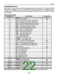
MEMORY
The DS2781 has a 256 byte linear memory space with registers for instrumentation, status, and control, as well as
EEPROM memory blocks to store parameters and user information. Byte addresses designated as “Reserved”
return undefined data when read. Reserved bytes should not be written. Several byte registers are paired into two-
byte registers in order to store 16-bit values. The most significant byte (MSB) of the 16 bit value is located at a
even address and the least significant byte (LSB) is located at the next address (odd) byte. When the MSB of a
two-byte register is read, the MSB and LSB are latched simultaneously and held for the duration of the Read Data
command to prevent updates to the LSB during the read. This ensures synchronization between the two register
bytes. For consistent results, always read the MSB and the LSB of a two-byte register during the same Read Data
command sequence.
EEPROM memory consists of the non-volatile EEPROM cells overlaid with volatile shadow RAM. The Read Data
and Write Data commands allow the 1-Wire interface to directly accesses only the shadow RAM. The Copy Data
and Recall Data function commands transfer data between the shadow RAM and the EEPROM cells. In order to
modify the data stored in the EEPROM cells, data must be written to the shadow RAM and then copied to the
EEPROM. In order to verify the data stored in the EEPROM cells, the EEPROM data must be recalled to the
shadow RAM and then read from the shadow RAM.
USER EEPROM
A 16 byte User EEPROM memory (block 0, addresses 20h–2Fh) provides non-volatile memory that is uncommitted
to other DS2781 functions. Accessing the User EEPROM block does not affect the operation of the DS2781. User
EEPROM is lockable, and once locked, write access is not allowed. The battery pack or host system manufacturer
can program lot codes, date codes and other manufacturing, warranty, or diagnostic information and then lock it to
safeguard the data. User EEPROM can also store parameters for charging to support different size batteries in a
host device as well as auxiliary model data such as time to full charge estimation parameters.
21 of 31

 MAXIM [ MAXIM INTEGRATED PRODUCTS ]