DS2781
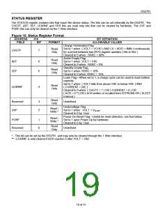
CONTROL REGISTER
All CONTROL register bits are read and write accessible. The CONTROL register is recalled from Parameter
EEPROM memory at power-up. Register bit values can be modified in shadow RAM after power-up. Shadow RAM
values can be saved as the power up default values by using the Copy Data command.
Figure 19. Control Register Format
ADDRESS
FIELD
60h
BIT
BIT DEFINITION
ALLOWABLE VALUES
FORMAT
Negative Blanking Enable
NBEN
7
Read/Write 0: Allows negative current readings to always be accumulated
1: Enables blanking of negative current readings up to -25µV
Under Voltage SLEEP Enable
0: Disables transition to SLEEP mode based on VIN voltage
1: Enables transition to SLEEP mode if,
UVEN
6
Read/Write
VIN < VSLEEP AND DQ stable at either logic level for tSLEEP
Power Mode Enable
PMOD
5
4
Read/Write 0: Disables transition to SLEEP mode based on DQ logic state
1: Enables transition to SLEEP mode if DQ at a logic-low for tSLEEP
Read Net Address Opcode
Read/Write 0: Read Net Address Command = 33h
1: Read Net Address Command = 39h
RNAOP
Under Voltage Threshold Select
UVTH
3
Read/Write 0: Selects an Under Voltage Sleep threshold of 2.45V
1: Selects an Under Voltage Sleep threshold of 4.9V
Reserved
0:2
—
Undefined
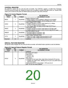
SPECIAL FEATURE REGISTER
All Special Feature Register bits are read and write accessible, with default values specified in each bit definition.
Figure 20. Special Feature Register Format
ADDRESS
FIELD
15h
BIT
BIT DEFINITION
ALLOWABLE VALUES
FORMAT
Reserved
1:7
—
Undefined
PIO Sense and Control
Read values
0: PIO pin ≤ Vil
1: PIO pin ≥ Vih
Write values
PIOSC
0
Read/Write
0: Activates PIO pin open-drain output driver, forcing the PIO pin low
1: Disables the output driver, allowing the PIO pin to be pulled high or
used as an input
Power-up and SLEEP mode default: 1 (PIO pin is hi-Z)
Note: PIO pin has weak pulldown
20 of 31

 MAXIM [ MAXIM INTEGRATED PRODUCTS ]