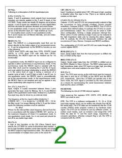
I/O Pins:
CNT_EN (Pin 13)
Following is a description of all the input/output pins.
Input. Counting is enabled when CNT_EN input is high; counting
is disabled when this input is low. There is an internal pull-up
resistor on this input.
A (Pin 12) B (Pin 11)
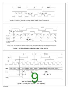
Inputs. A and B quadrature clock outputs from incremental
encoders are directly applied to the A and B inputs of the
LS7366R. These clocks are ideally 90 degrees out-of-phase
signals. A and B inputs are validated by on-chip digital filters
and then decoded for up/down direction and count clocks.
In non-quadrature mode, A serves as the count input and B
serves as the direction input (B = high enables up count,
B = low enables down count). In non-quadrature mode,
the A and B inputs are not filtered internally, and are instan-
taneous in nature.
LFLAG/ (Pin 8), DFLAG/ (Pin 9)
Outputs. LFLAG/ and DFLAG/ are programmable outputs to flag
the occurences of Carry (counter overflow), Borrow (counter
underflow), Compare (CNTR = DTR) and INDEX. The LFLAG/ is
an open drain latched output. In contrast, the DFLAG/ is a push-
pull instantaneous output. The LFLAG/ can be wired in multi-
slave configuration, forming a single processor interrupt line.
When active LFLAG/ switches to logic 0 and can be restored to
the high impedence state only by clearing the status register,
STR. In contrast, the DFLAG/ dynamically switches low with
occurences of Carry, Barrow, Compare and INDEX conditions.
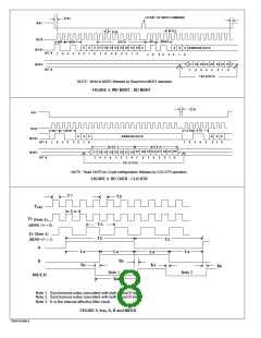
INDEX/ (Pin 10)
Input. The INDEX/ is a programmable input that can be
driven directly by the Index output of an incremental encod-
er. It can be programmed via the MDR0 to function as one
of the following:
The configuration of LFLAG/ and DFLAG/ are made through the
control register MDR1.
LCNTR (load CNTR with data from DTR), RCNTR (reset
CNTR), or LOTR (load OTR with data from CNTR).
Alternatively, the INDEX input can be masked out for "no
functionality".
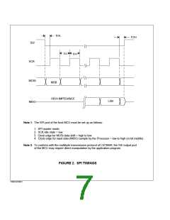
MOSI (RXD) (Pin 7)
Input. Serial output data from the host processor is shifted into
the LS7366R at this input.
MISO (TXD) (Pin 6)
In quadrature mode, the INDEX/ input can be configured to
operate in either synchronous or asynchronous mode. In the
synchronous mode the INDEX/ input is sampled with the
same filter clock used for sampling the A and the B inputs
and must satisfy the phase relationship in which the INDEX/
is in the active level of Logic 0 during a minimum of a
quarter cycle of both A and B High or both A and B Low. In
non-quadrature mode, the INDEX/ input is unconditionally
set to the asynchronous mode. In the asynchronous mode,
the INDEX/ input is not sampled and can be applied in any
phase relationship with respect to A and B.
Output. Serial output data from the LS7366R is shifted out on
the MISO (Master In Slave Out) pin. The MISO output goes into
high impedance state when SS/ input is at logic high, providing
multiple slave-unit serial outputs to be wire-ORed.
SCK (Pin 5)
Input. The SCK input serves as the shift clock input for transmit-
ting data in and out of LS7366R on the MOSI and the MISO
pins, respectively. Since the LS7366R can operate only in the
slave mode, the SCK signal is provided by the host processor
as a means for synchronizing the serial transmission between
itself and the slave LS7366R.
fCKi (Pin 2), fCK0 (Pin 1)
Input, Output. A crystal connected between these 2 pins
generates the basic clock for filtering the A, B and INDEX/
inputs in the quadrature count mode. Instead of a crystal the
fCKi input may also be driven by an external clock.
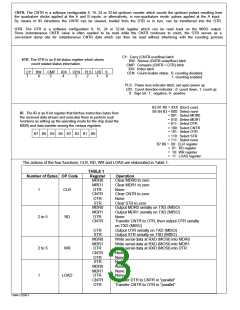
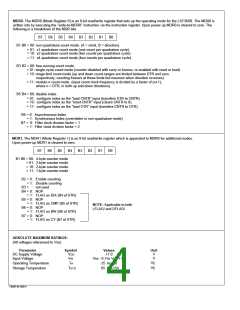
REGISTERS:
The following is a list of LS7366 internal registers:
Upon power-up the registers DTR, CNTR, STR, MDR0 and
MDR1 are reset to zero.
The frequency at the fCKi input is either divided by 2
(if MDR0 <B7> = 1) or divided by 1 (if MDR0 <B7> = 0) for
the filter circuit. For proper filtering of the A, B and the Index/
inputs the following condition must be satisfied:
DTR. The DTR is a software configurable 8, 16, 24 or 32-bit
input data register which can be written into directly from MOSI,
the serial input. The DTR data can be transferred into the 32-bit
counter (CNTR) under program control or by hardware index
signal. The DTR can be cleared to zero by software control. In
certain count modes, such as modulo-n and range-limit, DTR
holds the data for "n" and the count range, respectively. In
compare operations, whereby compare flag is set, the DTR is
compared with the CNTR.
ff ³ 4fQA
Where ff is the internal filter clock frequency derived from the
fCKi in accordance with the status of MDR0 <B7> and fQA is
the maximum frequency of Clock A in quadrature mode. In
non-quadrature count mode, fCKi is not used and should be
tied off to any stable logic state.
SS/ (Pin 4)
A high to low transition at the SS/ (Slave Select) input
selects the LS7366R for serial bi-directional data transfer; a
low to high transition disables serial data transfer and brings
the MISO output to high impedance state. This allows for the
accommodation of multiple slave units on the serial I/O.
7366R-050106-2

 LSI [ LSI COMPUTER SYSTEMS ]