LTC6103
APPLICATIONS INFORMATION
CMPZ4697
10k
V
LOGIC
(3.3V TO 5V)
M1
Si4465
7
LTC1540
3
4
5
6
R
R
SENSE(HI)
+
–
SENSE(LO)
100mΩ
I
LOAD
10mΩ
8
Q1
CMPT5551
V
V
IN
OUT
40.2k
1.74M
619k
4.7k
301Ω
301Ω
8
1
7
6
5
HIGH
RANGE
2
1
INDICATOR
LTC6103
4
(I
> 1.2A)
LOAD
HIGH CURRENT
RANGE OUT
250mV/A
2
BAT54C
7.5k
V
LOGIC
LOW CURRENT
RANGE OUT
250mV/A
6103 F03b
R5
7.5k
(V
0A ≤ I
+ 5V) ≤ V ≤ 60V
IN
LOGIC
≤ 10A
LOAD
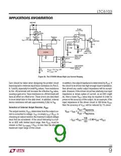
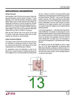
Figure 3b. The LTC6103 Allows High-Low Current Ranging
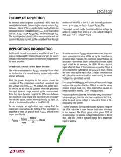
Care should be taken when designing the printed circuit
board layout to minimize input trace resistance (to Pins 5,
Inaddition,theoutputimpedanceisdeterminedbyR .If
OUT
the circuit to be driven has high enough input impedance,
then almost any useful output impedance will be accept-
able. However, if the driven circuit has relatively low input
impedance or draws spikes of current, as an ADC might
6,7and8),especiallyforsmallR values.Traceresistance
IN
to the –IN terminals will increase the effective R value,
IN
causingagainerror. Traceresistanceon+INterminalswill
have an effect on offset error. These errors are described
in more detail later in this data sheet. In addition, internal
do, then a lower R
value may be required in order to
OUT
preserve the accuracy of the output. As an example, if the
device resistance will add approximately 0.3Ω to R .
input impedance of the driven circuit is 100 times R
then the accuracy of V
,
OUT
IN
will be reduced by 1% since:
OUT
Selection of External Output Resistor, R
OUT
ROUT •RIN(DRIVEN)
VOUT = IOUT
•
The output resistor, R , determines how the output cur-
OUT
ROUT +RIN(DRIVEN)
rent is converted to voltage. V
is simply I • R . In
OUT OUT
OUT
choosing an output resistor, the maximum output voltage
must first be considered. If the circuit following is a buf-
100
101
= IOUT •ROUT
•
= 0.99 •IOUT •ROUT
fer or ADC with limited input range, then R
must be
OUT
chosen so that I
• R
is less than the allowed
OUT(MAX)
OUT
maximum input range of this circuit.
6103f
9

 Linear [ Linear ]