LTC7541A
ELECTRICAL CHARACTERISTICS
VDD = 15V, VREF = 10V, OUT 1 = OUT 2 = GND = 0V, TA = TMIN to TMAX, unless otherwise specified.
ALL GRADES
SYMBOL PARAMETER
Power Supply
CONDITIONS
MIN
TYP
MAX
UNIT
V
Operating Supply Range
Suppy Current
●
5
15
16
V
DD
I
Digital Inputs = V or V
●
●
2
100
mA
µA
DD
IH
IL
Digital Inputs = 0V or V
DD
Digital Inputs
V
V
Digital Input High Voltage
Digital Input Low Voltage
Digital Input Current
●
●
●
●
2.4
V
V
IH
IL
0.8
±1
8
I
0.001
µA
pF
IN
C
IN
Digital Input Capacitance
(Note 3), V = 0V
IN
AC Performance
Propagation Delay
(Notes 5, 6)
(Notes 5, 7)
100
1000
1.0
ns
Digital-to-Analog Glitch Impulse
Multiplying Feedthrough Error
Output Current Settling Time
Output Capacitance (Note 3)
nV-sec
V
= ±10V, 10kHz Sinewave
mV
P-P
REF
(Note 5), To 0.01% for Full-Scale Change
0.6
µs
C
OUT
Digital Inputs = V
C
C
●
●
200
70
pF
pF
IH
OUT1
OUT2
Digital Inputs = V
C
C
●
●
70
200
pF
pF
IL
OUT1
OUT2
The
●
denotes specifications which apply over the full operating
Note 5: OUT 1 load = 100Ω in parallel with 13pF.
Note 6: Measured from digital input change to 90% of final analog value.
Digital inputs = 0V to V or V to 0V.
temperature range.
Note 1: ±0.5LSB = ±0.012% of full scale.
Note 2: Using internal feedback resistor.
Note 3: Guaranteed by design, not subject to test.
DD
DD
Note 7: V = 0V. All digital inputs 0V to V or V to 0V. Measured
REF
DD
DD
using LT1363 as output amplifier.
Note 4: I
inputs = V
with all digital inputs = 0V or I
with all digital
OUT1
OUT2
.
DD
W
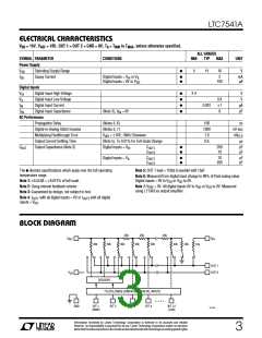
BLOCK DIAGRAM
20k
40k
20k
20k
V
R
FB
REF
40k
40k
40k
40k
40k
40k
10k
OUT 1
OUT 2
V
DD
DECODER
TTL/DTL/CMOS COMPATIBLE DIGITAL INPUTS
• • • •
GND
BIT 1
(MSB)
BIT 2
BIT 3
BIT 4
BIT 12
(LSB)
7541 BD
Information furnished by Linear Technology Corporation is believed to be accurate and reliable.
However, no responsibility is assumed for its use. Linear Technology Corporation makes no represen-
tationthattheinterconnectionofitscircuitsasdescribedhereinwillnotinfringeonexistingpatentrights.
3

 Linear [ Linear ]