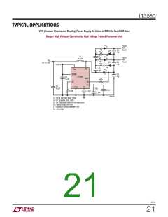
LT3580
APPLICATIONS INFORMATION
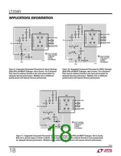
C2, for best load regulation. You can tie the local ground
into the system ground plane at the C3 ground terminal.
Board layout also has a significant effect on thermal re-
sistance. The exposed package ground pad is the copper
plate that runs under the LT3580 die. This is a good thermal
path for heat out of the package. Soldering the pad onto
theboardreducesdietemperatureandincreasesthepower
capability of the LT3580. Provide as much copper area as
possible around this pad. Adding multiple feedthroughs
around the pad to the ground plane will also help. Figures
9 and 10 show the recommended component placement
for the boost and SEPIC configurations, respectively.
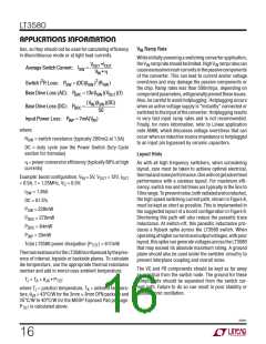
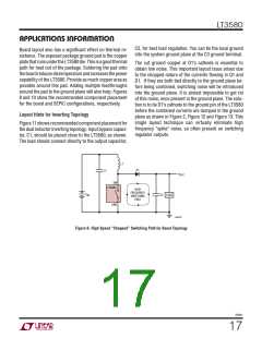
The cut ground copper at D1’s cathode is essential to
obtain low noise. This important layout issue arises due
to the chopped nature of the currents flowing in Q1 and
D1. If they are both tied directly to the ground plane be-
fore being combined, switching noise will be introduced
into the ground plane. It is almost impossible to get rid
of this noise, once present in the ground plane. The solu-
tion is to tie D1’s cathode to the ground pin of the LT3580
before the combined currents are dumped in the ground
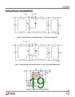
plane as drawn in Figure 2, Figure 12 and Figure 13. This
single layout technique can virtually eliminate high
frequency “spike” noise, so often present on switching
regulator outputs.
Layout Hints for Inverting Topology
Figure 11 shows recommended component placement for
the dual inductor inverting topology. Input bypass capaci-
tor, C1, should be placed close to the LT3580, as shown.
The load should connect directly to the output capacitor,
L1
D1
C1
V
OUT
SW
LT3580
HIGH
FREQUENCY
SWITCHING
PATH
V
IN
C2 LOAD
GND
3580 F08
Figure 8. High Speed “Chopped” Switching Path for Boost Topology
3580fc
17

 Linear [ Linear ]