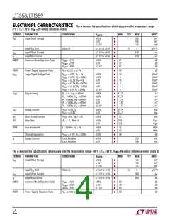
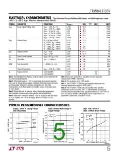
LT1358/LT1359
U
W U U
APPLICATIONS INFORMATION
BecauseofvariationinthematchingofNPNandPNPbeta,
the polarity of the input bias current can be positive or
negative. The offset current does not depend on NPN/PNP
beta matching and is well controlled. The use of balanced
source resistance at each input is recommended for
applications where DC accuracy must be maximized.
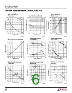
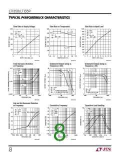
greater input step. The curve of Slew Rate vs Input Level
illustratesthisrelationship.TheLT1358/LT1359aretested
for slew rate in a gain of –2 so higher slew rates can be
expected in gains of 1 and –1, and lower slew rates in
higher gain configurations.
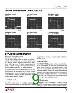
The RC network across the output stage is bootstrapped
when the amplifier is driving a light or moderate load and
has no effect under normal operation. When driving a
capacitive load (or a low value resistive load) the network
is incompletely bootstrapped and adds to the compensa-
tion at the high impedance node. The added capacitance
slows down the amplifier which improves the phase
margin by moving the unity-gain frequency away from the
pole formed by the output impedance and the capacitive
load. The zero created by the RC combination adds phase
to ensure that even for very large load capacitances, the
total phase lag can never exceed 180 degrees (zero phase
margin) and the amplifier remains stable.
The inputs can withstand transient differential input volt-
ages up to 10V without damage and need no clamping or
source resistance for protection. Differential inputs, how-
ever, generate large supply currents (tens of mA) as
required for high slew rates. If the device is used with
sustained differential inputs, the average supply current
will increase, excessive power dissipation will result and
the part may be damaged. The part should not be used as
acomparator,peakdetectororotheropen-loopapplica-
tion with large, sustained differential inputs. Under
normal, closed-loop operation, an increase of power dis-
sipationisonlynoticeableinapplicationswithlargeslewing
outputs and is proportional to the magnitude of the
differential input voltage and the percent of the time that
the inputs are apart. Measure the average supply current
for the application in order to calculate the power dissipa-
tion.
Power Dissipation
TheLT1358/LT1359combinehighspeedandlargeoutput
drive in small packages. Because of the wide supply
voltage range, it is possible to exceed the maximum
junction temperature under certain conditions. Maximum
junction temperature (TJ) is calculated from the ambient
temperature (TA) and power dissipation (PD) as follows:
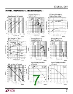
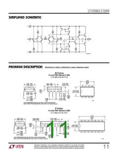
Circuit Operation
The LT1358/LT1359 circuit topology is a true voltage
feedback amplifier that has the slewing behavior of a
currentfeedbackamplifier.Theoperationofthecircuitcan
be understood by referring to the simplified schematic.
The inputs are buffered by complementary NPN and PNP
emitter followers which drive a 500Ω resistor. The input
voltage appears across the resistor generating currents
whicharemirroredintothehighimpedancenode.Comple-
mentary followers form an output stage which buffers the
gain node from the load. The bandwidth is set by the input
resistor and the capacitance on the high impedance node.
The slew rate is determined by the current available to
charge the gain node capacitance. This current is the
differential input voltage divided by R1, so the slew rate is
proportional to the input. Highest slew rates are therefore
seen in the lowest gain configurations. For example, a 10V
output step in a gain of 10 has only a 1V input step,
whereas the same output step in unity gain has a 10 times
LT1358CN8: TJ = TA + (PD x 130°C/W)
LT1358CS8: TJ = TA + (PD x 190°C/W)
LT1359CN: TJ = TA + (PD x 110°C/W)
LT1359CS: TJ = TA + (PD x 150°C/W)
Worst case power dissipation occurs at the maximum
supply current and when the output voltage is at 1/2 of
either supply voltage (or the maximum swing if less than
1/2 supply voltage). For each amplifier PDMAX is:
PDMAX = (V+ – V–)(ISMAX) + (V+/2)2/RL
Example: LT1358 in S8 at 70°C, VS = ±15V, RL = 500Ω
PDMAX = (30V)(2.9mA) + (7.5V)2/500Ω = 200mW
TJMAX = 70°C + (2 x 200mW)(190°C/W) = 146°C
10

 Linear [ Linear ]