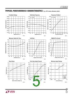
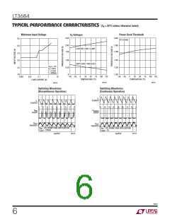
LT3684
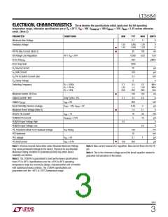
ELECTRICAL CHARACTERISTICS
noted. (Note 2)
The
●
denotes the specifications which apply over the full operating
= 10V V = 15V, V = 3.3V unless otherwise
temperature range, otherwise specifications are at T = 25°C. V = 10V, V
A
IN
RUNS/SS
BOOST
BIAS
MIN
PARAMETER
CONDITIONS
TYP
MAX
UNITS
Minimum Bias Voltage
Feedback Voltage
2.7
3
V
1.25
1.24
1.265
1.265
1.28
1.29
V
V
●
●
FB Pin Bias Current (Note 3)
FB Voltage Line Regulation
30
0.002
330
1000
75
100
nA
%/V
4V < V < 34V
0.02
IN
Error Amp g
µMho
m
Error Amp Gain
V Source Current
µA
µA
A/V
V
C
V Sink Current
C
100
3.5
V Pin to Switch Current Gain
C
V Clamp Voltage
C
2
Switching Frequency
R = 8.66k
2.7
1.25
250
3.0
1.4
300
3.3
1.55
350
MHz
MHz
kHz
T
R = 29.4k
T
R = 187k
T
●
●
Minimum Switch Off-Time
Switch Current Limit
100
3.6
360
0.02
1.6
18
150
4.0
nS
A
Duty Cycle = 5%
3.1
Switch V
I
= 2A
SW
mV
µA
V
CESAT
Boost Schottky Reverse Leakage
Minimum Boost Voltage (Note 4)
BOOST Pin Current
V
SW
= 10V, V
= 0V
BIAS
2
2.1
30
10
I
SW
= 1A
mA
µA
V
RUN/SS Pin Current
V
= 2.5V
5
RUN/SS
RUN/SS Input Voltage High
RUN/SS Input Voltage Low
PG Threshold Offset from Feedback Voltage
PG Hysteresis
2.5
0.2
1
V
V
FB
Rising
100
10
mV
mV
µA
µA
PG Leakage
V
V
= 5V
0.1
300
PG
●
PG Sink Current
= 0.4V
100
PG
Note 1: Stresses beyond those listed under Absolute Maximum Ratings
may cause permanent damage to the device. Exposure to any Absolute
Maximum Rating condition for extended periods may affect device
reliability and lifetime.
Note 3: Bias current measured in regulation. Bias current flows into the FB
pin.
Note 4: This is the minimum voltage across the boost capacitor needed to
guarantee full saturation of the switch.
Note 2: The LT3684E is guaranteed to meet performance specifications
from 0°C to 85°C. Specifications over the –40°C to 85°C operating
temperature range are assured by design, characterization and correlation
with statistical process controls. The LT3684I specifications are
guaranteed over the –40°C to 125°C temperature range.
3684f
3

 Linear [ Linear ]