LT3681
W W U W
U
W
U
ABSOLUTE AXI U RATI GS
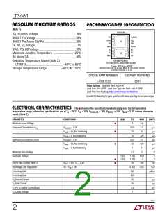
PACKAGE/ORDER I FOR ATIO
(Note 1)
TOP VIEW
V , RUN/SS Voltage.................................................36V
IN
PG
BIAS
FB
1
2
3
4
5
6
7
14 RUN/SS
13
BOOST Pin Voltage ...................................................56V
BOOST Pin Above SW Pin.........................................30V
V
IN
15
16
12 SW
FB, RT, V Voltage.......................................................5V
C
GND
11 BOOST
10 BD
BIAS, PG, BD Voltage................................................30V
Maximum Junction Temperature .......................... 125°C
DC above DA.............................................................40V
Operating Temperature Range (Note 2)
V
C
R
9
8
DC
DA
T
GND
DE14MA PACKAGE
14-LEAD (4mm 3mm) PLASTIC DFN
= 125°C, θ = 43°C/W
LT3681E............................................... –40°C to 85°C
Storage Temperature Range................... –65°C to 150°C
T
JMAX
JA
EXPOSED PAD (PIN 15) IS GND, MUST BE SOLDERED TO PCB
EXPOSED PAD PIN 16 IS DC
ORDER PART NUMBER
DE PART MARKING
3681
LT3681EDE
Order Options Tape and Reel: Add #TR
Lead Free: Add #PBF Lead Free Tape and Reel: Add #TRPBF
Lead Free Part Marking: http://www.linear.com/leadfree/
Consult LTC Marketing for parts specified with wider operating temperature ranges.
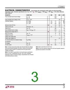
ELECTRICAL CHARACTERISTICS The
noted. (Note 2)
●
denotes the specifications which apply over the full operating
temperature range, otherwise specifications are at T = 25°C. V = 10V, V
= 10V, V
= 15V, V
= 3.3V unless otherwise
BIAS
A
IN
RUNS/SS
BOOST
PARAMETER
CONDITIONS
MIN
TYP
3
MAX
3.6
0.5
60
UNITS
V
●
●
Minimum Input Voltage
Quiescent Current from V
V
V
V
V
V
V
= 0.2V
0.01
22
μA
μA
μA
μA
μA
μA
V
IN
RUN/SS
= 3V, Not Switching
= 0, Not Switching
BIAS
75
120
0.5
120
5
BIAS
Quiescent Current from BIAS
= 0.2V
0.01
50
RUN/SS
●
= 3V, Not Switching
= 0, Not Switching
BIAS
BIAS
0
Minimum Bias Voltage
Feedback Voltage
2.7
3
1.25
1.24
1.265
1.265
1.29
1.3
V
V
●
●
FB Pin Bias Current (Note 3)
FB Voltage Line Regulation
Error Amp GM
V
FB
= 1.25V, V = 0.4V
30
0.002
330
800
65
100
nA
%/V
C
4V < V < 34V
0.02
IN
μMho
Error Amp Gain
V Source Current
C
μA
μA
A/V
V
V Sink Current
C
85
V Pin to Switch Current Gain
C
3.5
2
V Clamp Voltage
C
3681f
2

 Linear [ Linear ]