LT3518
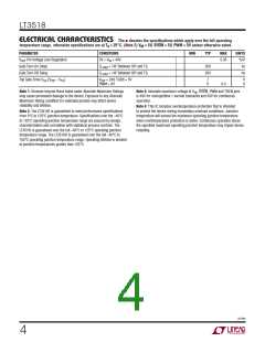
ELECTRICAL CHARACTERISTICS The l denotes the specifications which apply over the full operating
temperature range, otherwise specifications are at TA = 25°C. (Note 2) VIN = 5V, SHDN = 5V, PWM = 5V unless otherwise noted.
PARAMETER
Pin Voltage Line Regulation
CONDITIONS
3V < V < 40V
MIN
TYP
MAX
UNITS
%/V
ns
V
REF
0.03
IN
Gate Turn-On Delay
Gate Turn-Off Delay
C
C
V
= 1nF Between ISP and TG
= 1nF Between ISP and TG
200
200
LOAD
LOAD
ns
Top Gate Drive V (V – V
)
TG
= 24V, TGEN = 5V
ISP
7
0
V
V
GS ISP
PWM = 0V
0.3
Note 1: Stresses beyond those listed under Absolute Maximum Ratings
may cause permanent damage to the device. Exposure to any Absolute
Maximum Rating condition for extended periods may affect device
reliability and lifetime.
Note 2: The LT3518E is guaranteed to meet performance specifications
from 0°C to 125°C junction temperature. Specifications over the –40°C
to 125°C operating junction temperature range are assured by design,
characterization and correlation with statistical process controls. The
LT3518I is guaranteed over the full –40°C to 125°C operating junction
temperature range. The LT3518H is guaranteed over the full –40°C to
150°C operating junction temperature range. Operating lifetime is derated
at junction temperatures greater than 125°C.
Note 3: Absolute maximum voltage at V , SHDN, PWM and TGEN pins
is 40V for nonrepetitive 1 second transients and 30V for continuous
operation.
Note 4: This IC includes overtemperature protection that is intended
to protect the device during momentary overload conditions. Junction
temperature will exceed the maximum operating junction temperature
when overtemperature protection is active. Continuous operation above
the specified maximum operating junction temperature may impair device
reliability.
IN
3518fb
4

 Linear [ Linear ]