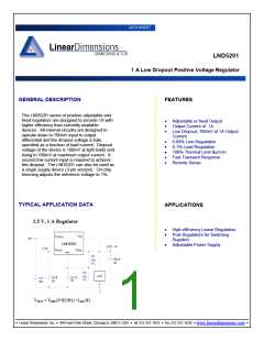
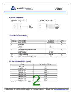
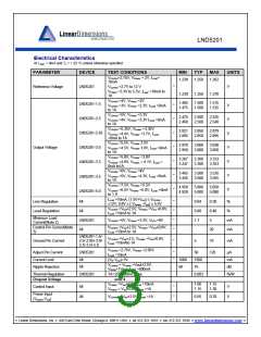
LND5201
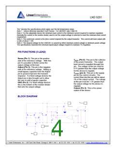
Output Voltage
Protection Diodes
The LND5201 (adjustable version)
develops a 1.25V reference voltage
between the Sense pin and the Adjust
pin (Figure 4). Placing a resistor
between these two terminals causes a
constant current to flow through R1 and
down though R2 to set the output
voltage. In general R1 is chosen so that
this current is the specified minimum
load current of 5mA. The current out of
the Adjust pin is small, typically 50µA
and it adds to the current from R1. For
the best regulation the top of the resistor
divider should be connected directly to
the Sense pin.
In normal operation LND5201 family does
not need any protection diodes between
the adjustment pin and the output to the
input to prevent die overstresses. Internal
resistors are limiting the internal current
paths on the ADJ pin. Therefore even
with bypass capacitors on the adjust pin
no protection diode is needed to ensure
device safety under short-circuit
conditions. The adjust pin can be driver
on a transient basis ±7V with respect to
the output with out any device
degradation. A protection diode between
the Output pin and Vpower pin is not
usually needed. Microsecond surge
currents of 50A to 100A can be handled
by the internal diode between the Output
pin and Vpower pin of the device. In
normal operations it is difficult to get those
values of surge currents even with the
use of large output capacitance. Only
with high value output capacitors, such as
1000 to 5000µF and the Vpower pin are
instantaneously shorted to ground,
damage can occur. A diode from output
to input is recommended (Figure 5).
If LND5201 is connected as a single
supply device with the control and power
input pins shorted together the internal
diode between the output and the power-
input pin will protect the control input pin.
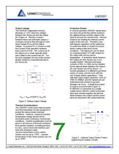
VOUT = VREF (I+R2/R1) +IADJ R2
Figure 4. Setting Output Voltage
Thermal Considerations
The LND5201 series have internal power
and thermal-limiting circuitry designed to
protect the device under overload
conditions. However, maximum junction
temperature ratings should not be
exceeded under continuous normal load
conditions. Careful consideration must be
given to all sources of thermal resistance
from junction ambient, including junction-
to-case, case to-heat sink interface and
heat sink resistance itself.
Junction temperature of the control
section can run up to 125ºC. Junction
temperature of the Power section can run
up to 150ºC.
Figure 5. Optional Clamp Diodes Protect
Against Input Crowbar Circuits.
• Linear Dimensions, Inc. • 445 East Ohio Street, Chicago IL 60611 USA • tel 312.321.1810 • fax 312.321.1830 • www.lineardimensions.com •

 LINEAR_DIMENSIONS [ Linear Dimensions ]