LND1117
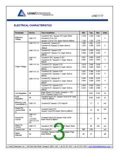
Parameter
Device
Test Conditions
A = 25ºC,30ms pulse
Min
Typ
Max
Units
Thermal
Regulation
LND1117
T
0.003
%/W
Dropout Voltage
Control Input
(Vcontrol-Vout)
Power Input
Vpower=Vout+0.8V, Iload=10mA
Vpower=Vout+0.8V, Iload=800mA
1.00
1.15
1.15
1.30
All
All
*
*
V
V
Vcontrol= Vout+2.5V, Iload=800mA
0.55
0.70
(Vpower-Vout)
The *denotes the specifications which apply over the full temperature range.
Note 1: Unless otherwise specified Vout=Vsense. For LND1117(adj) Vadj=OV
Note 2: For the adjustable device the minimum load current is the minimum current required to maintain regulation. Normally the
current in the resistor divider used to set the output voltage is selected to meet the minimum load current requirement.
Note3: The control pin current is the drive current required for the output transistor. The current will track output current with a ratio of
about 1:100.
Note4: The dropout voltage for the LND1117 is caused by either minimum control voltage or minimum power voltage. The
specifications represent the minimum input/output voltage required to maintain 1% regulation.
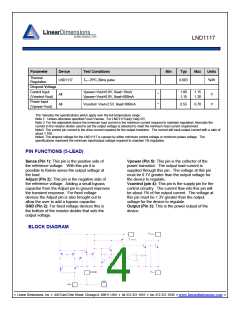
PIN FUNCTIONS (5-LEAD)
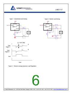
Sense (Pin 1): This pin is the positive side of
the reference voltage. With this pin it is
possible to Kelvin sense the output voltage at
the load.
Adjust (Pin 2): This pin is the negative side of
the reference voltage. Adding a small bypass
capacitor from the Adjust pin to ground improves
the transient response. For fixed voltage
devices the Adjust pin is also brought out to
allow the user to add a bypass capacitor.
GND (Pin 2): For fixed voltage devices this is
the bottom of the resistor divider that sets the
output voltage.
Vpower (Pin 5): This pin is the collector of the
power transistor. The output load current is
supplied through this pin. The voltage at this pin
must be 0.7V greater than the output voltage for
the device to regulate.
Vcontrol (pin 4): This pin is the supply pin for the
control circuitry. The current flow into this pin will
be about 1% of the output current. The voltage at
this pin must be 1.3V greater than the output
voltage for the device to regulate.
Output (Pin 3): This is the power output of the
device.
BLOCK DIAGRAM
• Linear Dimensions, Inc. • 445 East Ohio Street, Chicago IL 60611 USA • tel 312.321.1810 • fax 312.321.1830 • www.lineardimensions.com •

 LINEAR_DIMENSIONS [ Linear Dimensions ]