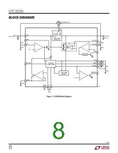
LTC3226
APPLICATIONS INFORMATION
So even if the charge pump input current limit is pro-
Supercapacitor Manufacturers
grammed for 315mA (R
= 33.2k), the actual charge
PROG
Refer to the following table for supercapacitor manu-
facturers.
current will be considerably less than 157.5mA (half of
programmed limit) in 2x mode for very low input supply.
Table 1. Supercapacitor Manufacturers
For V = 2.5V, the CPO voltage above which the charge
IN
current will decrease from the programmed value of
CAP-XX
www.cap-xx.com
157.5mA (R
= 33.2k) can be calculated from the
NESS CAP
Maxwell
www.nesscap.com
PROG
previous equation as follows:
www.maxwell.com
Bussmann
AVX
www.cooperbussmann.com
www.avx.com
V
= (2 • 2.5V – 157.5mA • 6Ω) = 4.055V
CPO
Illinois Capacitor
Tecate Group
www.illinoiscapacitor.com
www.tecategroup.com
Choosing the LDO Output Capacitor
IntheeventV fallsbelowtheprogrammedPFIthreshold,
IN
the PFI comparator turns off the charge pump and turns
on the internal LDO to supply the load from the backed-
up supercapacitor storage. However, due to the delay
associated with the PFI comparator and LDO circuitry, it
could be up to 2μs before the LDO is capable of supplying
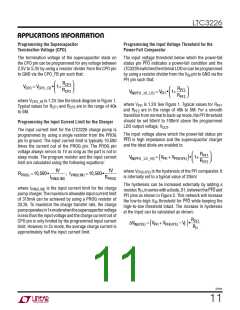
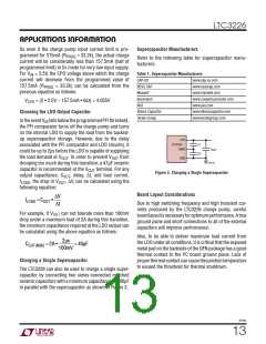
CPO
LTC3226
C1
C
VMID
SUP
C2
the load demand at V . In order to prevent V
from
GND
OUT
OUT
3226 F03
drooping too much during this transition, a 47μF ceramic
capacitor is recommended at the V terminal. For any
OUT
Figure 3. Charging a Single Supercapacitor
output capacitance, C , delay, Δt, and load current,
OUT
I
, the drop in V , ∆V, can be calculated using the
LOAD
OUT
following equation:
Board Layout Considerations
ΔV
Δt
ILOAD =COUT
•
Due to high switching frequency and high transient cur-
rents produced by the LTC3226 charge pump, careful
boardlayoutisnecessaryforoptimumperformance.Atrue
ground plane and short connections to all of the external
capacitors will improve performance.
For example, if V
can not tolerate more than 100mV
OUT
drop under a maximum load of 2A during this transition,
the minimum capacitance required at the LDO output can
be calculated using the above equation as follows:
Also, to be able to deliver maximum load current from
the LDO under all conditions, it is critical that the exposed
metal pad on the backside of the QFN package has a good
thermal contact to the PC board ground plane. Lack of
properthermalcontactcancausethejunctiontemperature
to exceed the threshold for thermal shutdown.
2µs
100mV
COUT(MIN) = 2A •
= 40µF
Charging a Single Supercapacitor
The LTC3226 can also be used to charge a single super-
capacitor by connecting two series-connected matched
ceramic capacitors with a minimum capacitance of 100ꢀF
in parallel with the supercapacitor as shown in Figure 3.
3226fa
13

 Linear Systems [ Linear Systems ]