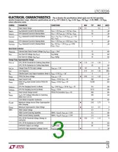
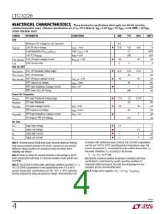
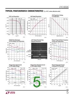
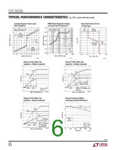
LTC3226
PIN FUNCTIONS
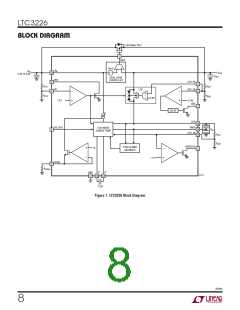
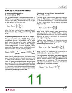
PROG (Pin 9): Charger Input Current Limit Programming
Pin. A resistor connected between this pin and GND sets
the input current limit for the charger. See the Applications
Information section.
V
(Pin 1): Voltage Output. This pin is used to provide
OUT
power to an external load from either the primary input
supply (V ) or the supercapacitor (CPO) if the primary
IN
input supply is not available. V
should be bypassed
OUT
with a low ESR ceramic capacitor of at least 47ꢀF capaci-
CPO_FB (Pin 10): Feedback Pin for the Charge Pump. The
voltage on this pin is compared to the internal reference
voltage (1.2V) to keep the charge pump output CPO in
regulation.Anexternalresistordividerisrequiredbetween
CPO, CPO_FB and GND to program the CPO output volt-
age. See the Applications Information section.
tance to GND.
PFO (Pin 2): Open-Drain Power-Fail Status Output. This
pin is pulled to ground by an internal N-channel MOSFET
when the PFI input is below 1.2V. Once the PFI input re-
covers, this pin becomes high impedance.
CAPGOOD (Pin 11): Open-Drain Status Output of the
CPO Voltage. This pin is pulled to ground by an internal
N-channel MOSFET until CPO_FB pin reaches 1.11V. Once
the CPO_FB pin exceeds 1.11V, this pin becomes high
impedance indicating that the CPO voltage is within 7.5%
of its target value.
PFI (Pin 3): Power-Fail Input. High impedance input to
an accurate comparator with a 1.2V falling threshold and
20mV hysteresis. This pin controls the state of the PFO
output pin and the operating mode of the LTC3226.
LDO_FB (Pin 4): Internal LDO Feedback Pin. The voltage
on this pin is compared to the internal reference voltage
(0.8V) by the error amplifier to keep the output in regula-
–
C (Pin 12): Internal Charge Pump Flying Capacitor
Negative Terminal.
tion.AnexternalresistordividerisrequiredbetweenV
,
OUT
LDO_FBandGNDtoprogramtheLDOoutputvoltage. See
the Applications Information section.
V (Pin13):PrimaryInputSupply.Thispinsuppliespower
IN
to the V
pin through an external P-channel MOSFET
OUT
and also to the supercapacitors attached to the CPO and
GATE (Pin 5): External FET Gate Pin. This pin is driven
VMID pins. V should be bypassed to GND with a low
by an internal ideal diode controller to regulate V
to
IN
OUT
ESR ceramic capacitor of at least 2.2μF depending on the
15mV below V .
IN
load transient.
RST_FB (Pin 6): Reset Comparator Input. High imped-
ance input to an accurate comparator with a 0.74V falling
threshold and 20mV hysteresis. This pin controls the
state of the RST output pin. An external resistor divider
VMID (Pin 14): Midpoint of Two Series Supercapacitors.
+
C (Pin15):InternalChargePumpFlyingCapacitorPositive
Terminal. A 1μF to 10μF X5R or X7R ceramic capacitor
is required between V , RST_FB and GND. It can be
+
–
OUT
should be connected from C to C .
the same resistor divider as the LDO_FB divider. See the
CPO (Pin 16): Backup Supply Pin. Connect CPO to the top
Applications Information section.
plate of the top supercapacitor. This pin receives power
RST (Pin 7): Open-Drain Status Output of the RESET
Comparator. This pin is pulled to ground by an internal
N-channelMOSFETwhenevertheRST_FBpinvoltagefalls
below 0.74V. Once the RST_FB pin voltage recovers, the
pin becomes high impedance after a 290ms delay indicat-
from V through an internal charge pump doubler and
IN
supplies power to V
primary input supply has failed.
through an internal LDO when the
OUT
GND (Exposed Pad Pin 17): Ground. The exposed pad
should be connected to a continuous ground plane on
the second layer of the printed circuit board by several
vias directly under the part to achieve optimal thermal
performance.
ing that V
is within 7.5% of its programmed value.
OUT
EN_CHG (Pin 8): Enable Pin for the Charge Pump Super-
capacitor Charger with an Internal Pull-Up. Tie this pin to
a voltage below 0.4V to disable the internal charge pump.
3226fa
7

 Linear Systems [ Linear Systems ]